NTTFS024N06C. Аналоги и основные параметры
Наименование производителя: NTTFS024N06C
Тип транзистора: MOSFET
Полярность: N
Предельные значения
Pd ⓘ
- Максимальная рассеиваемая мощность: 28 W
|Vds|ⓘ - Максимально допустимое напряжение сток-исток: 60 V
|Vgs|ⓘ - Максимально допустимое напряжение затвор-исток: 20 V
|Id| ⓘ - Максимально допустимый постоянный ток стока: 24 A
Tj ⓘ - Максимальная температура канала: 175 °C
Электрические характеристики
tr ⓘ -
Время нарастания: 1.3 ns
Cossⓘ - Выходная емкость: 225 pf
RDSonⓘ - Сопротивление сток-исток открытого транзистора: 0.0226 Ohm
Тип корпуса: WDFN8
Аналог (замена) для NTTFS024N06C
- подборⓘ MOSFET транзистора по параметрам
NTTFS024N06C даташит
..1. Size:141K onsemi
nttfs024n06c.pdf 
MOSFET - Power, Single N-Channel, m8FL 60 V, 22.6 mW, 24 A NTTFS024N06C Features www.onsemi.com Small Footprint (3.3 x 3.3 mm) for Compact Design Low RDS(on) to Minimize Conduction Losses Low QG and Capacitance to Minimize Driver Losses V(BR)DSS RDS(on) MAX ID MAX These Devices are Pb-Free, Halogen Free/BFR Free and are RoHS Compliant 60 V 22.6 mW @ 10 V 24 A Typica
7.1. Size:198K onsemi
nttfs020n06c.pdf 
MOSFET - Power, Single N-Channel, m8FL 60 V, 20.3 mW, 27 A NTTFS020N06C Features www.onsemi.com Small Footprint (3.3 x 3.3 mm) for Compact Design Low RDS(on) to Minimize Conduction Losses Low QG and Capacitance to Minimize Driver Losses V(BR)DSS RDS(on) MAX ID MAX These Devices are Pb-Free, Halogen Free/BFR Free and are RoHS Compliant 60 V 20.3 mW @ 10 V 27 A Typica
8.1. Size:205K onsemi
nttfs004n04c.pdf 
NTTFS004N04C MOSFET Power, Single, N-Channel 40 V, 4.9 mW, 77 A Features www.onsemi.com Small Footprint (3.3 x 3.3 mm) for Compact Design Low RDS(on) to Minimize Conduction Losses Low Capacitance to Minimize Driver Losses These Devices are Pb-Free and are RoHS Compliant V(BR)DSS RDS(on) MAX ID MAX 40 V 4.9 mW @ 10 V 77 A MAXIMUM RATINGS (TJ = 25 C unless otherwis
8.2. Size:201K onsemi
nttfs015p03p8z.pdf 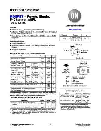
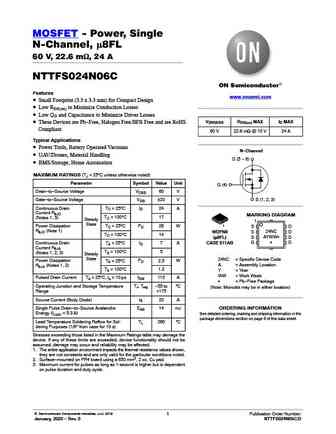
NTTFS015P03P8Z MOSFET Power, Single, P-Channel, m8FL -30 V, 7.5 mW Features www.onsemi.com Ultra Low RDS(on) to Improve System Efficiency Advanced Package Technology in 3.3x3.3mm for Space Saving and Excellent Thermal Conduction V(BR)DSS RDS(on) ID These Devices are Pb-Free, Halogen Free/BFR Free and are RoHS 7.5 mW @ -10 V Compliant -30 V -47.6 A 12 mW @ -4.5 V
8.3. Size:193K onsemi
nttfs005n04c.pdf 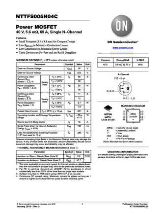
NTTFS005N04C Power MOSFET 40 V, 5.6 mW, 69 A, Single N-Channel Features Small Footprint (3.3 x 3.3 mm) for Compact Design Low RDS(on) to Minimize Conduction Losses www.onsemi.com Low Capacitance to Minimize Driver Losses These Devices are Pb-Free and are RoHS Compliant V(BR)DSS RDS(on) MAX ID MAX MAXIMUM RATINGS (TJ = 25 C unless otherwise noted) Parameter Symbol Val
8.4. Size:139K onsemi
nttfs016n06c.pdf 
MOSFET - Power, Single N-Channel, m8FL 60 V, 16.3 mW, 32 A NTTFS016N06C Features www.onsemi.com Small Footprint (3.3 x 3.3 mm) for Compact Design Low RDS(on) to Minimize Conduction Losses Low QG and Capacitance to Minimize Driver Losses V(BR)DSS RDS(on) MAX ID MAX These Devices are Pb-Free, Halogen Free/BFR Free and are RoHS Compliant 60 V 16.3 mW @ 10 V 32 A Typica
8.5. Size:199K onsemi
nttfs030n06c.pdf 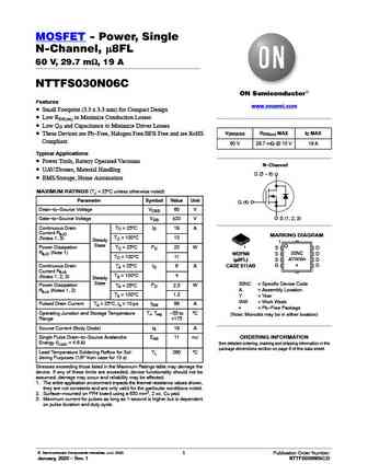
MOSFET - Power, Single N-Channel, m8FL 60 V, 29.7 mW, 19 A NTTFS030N06C Features www.onsemi.com Small Footprint (3.3 x 3.3 mm) for Compact Design Low RDS(on) to Minimize Conduction Losses Low QG and Capacitance to Minimize Driver Losses V(BR)DSS RDS(on) MAX ID MAX These Devices are Pb-Free, Halogen Free/BFR Free and are RoHS Compliant 60 V 29.7 mW @ 10 V 19 A Typica
8.6. Size:188K onsemi
nttfs008n04c.pdf 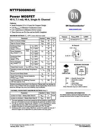
NTTFS008N04C Power MOSFET 40 V, 7.1 mW, 48 A, Single N-Channel Features Small Footprint (3.3 x 3.3 mm) for Compact Design Low RDS(on) to Minimize Conduction Losses www.onsemi.com Low Capacitance to Minimize Driver Losses These Devices are Pb-Free and are RoHS Compliant MAXIMUM RATINGS (TJ = 25 C unless otherwise noted) V(BR)DSS RDS(on) MAX ID MAX Parameter Symbol Val
8.7. Size:196K onsemi
nttfs003n04c.pdf 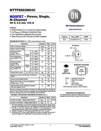
NTTFS003N04C MOSFET Power, Single, N-Channel 40 V, 3.5 mW, 103 A Features www.onsemi.com Small Footprint (3.3 x 3.3 mm) for Compact Design Low RDS(on) to Minimize Conduction Losses Low Capacitance to Minimize Driver Losses These Devices are Pb-Free and are RoHS Compliant V(BR)DSS RDS(on) MAX ID MAX 40 V 3.5 mW @ 10 V 103 A MAXIMUM RATINGS (TJ = 25 C unless otherw
8.8. Size:199K onsemi
nttfs015n04c.pdf 
NTTFS015N04C MOSFET Power, Single, N-Channel 40 V, 17.3 mW, 27 A Features www.onsemi.com Small Footprint (3.3 x 3.3 mm) for Compact Design Low RDS(on) to Minimize Conduction Losses Low Capacitance to Minimize Driver Losses These Devices are Pb-Free and are RoHS Compliant V(BR)DSS RDS(on) MAX ID MAX 40 V 17.3 mW @ 10 V 27 A MAXIMUM RATINGS (TJ = 25 C unless otherw
8.9. Size:355K onsemi
nttfs002n04cl.pdf 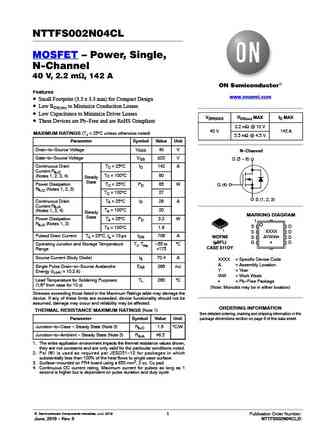
NTTFS002N04CL MOSFET Power, Single, N-Channel 40 V, 2.2 mW, 142 A Features www.onsemi.com Small Footprint (3.3 x 3.3 mm) for Compact Design Low RDS(on) to Minimize Conduction Losses Low Capacitance to Minimize Driver Losses V(BR)DSS RDS(on) MAX ID MAX These Devices are Pb-Free and are RoHS Compliant 2.2 mW @ 10 V 40 V 142 A MAXIMUM RATINGS (TJ = 25 C unless oth
8.10. Size:387K onsemi
nttfs010n10mcl.pdf 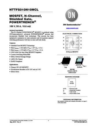
NTTFS010N10MCL MOSFET, N-Channel, Shielded Gate, POWERTRENCH) 100 V, 50 A, 10.6 mW www.onsemi.com General Description This N-Channel POWETRENCH MOSFET is produced using ELECTRICAL CONNECTION ON Semiconductor s advanced POWERTRENCH process that incorporates Shielded Gate technology. This process has been S D optimized to minimize on-state resistance and yet maintain superior
8.11. Size:272K onsemi
nttfs002n04c.pdf 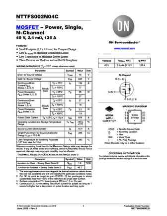
NTTFS002N04C MOSFET Power, Single, N-Channel 40 V, 2.4 mW, 136 A Features www.onsemi.com Small Footprint (3.3 x 3.3 mm) for Compact Design Low RDS(on) to Minimize Conduction Losses Low Capacitance to Minimize Driver Losses These Devices are Pb-Free and are RoHS Compliant V(BR)DSS RDS(on) MAX ID MAX 40 V 2.4 mW @ 10 V 136 A MAXIMUM RATINGS (TJ = 25 C unless other
Другие IGBT... NTTFS004N04C, NTTFS005N04C, NTTFS008N04C, NTTFS010N10MCL, NTTFS015N04C, NTTFS015P03P8Z, NTTFS016N06C, NTTFS020N06C, 18N50, NTTFS030N06C, NTTFS1D2N02P1E, NTTFS2D8N04HL, NTTFS4C02N, NTTFS5C453NL, NTTFS5C454NL, NTTFS5C460NL, NTTFS5C466NL
