NVMFD6H846NL Specs and Replacement
Type Designator: NVMFD6H846NL
Type of Transistor: MOSFET
Type of Control Channel: N-Channel
Absolute Maximum Ratings
Pd ⓘ
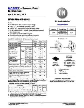
- Maximum Power Dissipation: 34 W
|Vds|ⓘ - Maximum Drain-Source Voltage: 80 V
|Vgs|ⓘ - Maximum Gate-Source Voltage: 20 V
|Id| ⓘ - Maximum Drain Current: 31 A
Tj ⓘ - Maximum Junction Temperature: 175 °C
Electrical Characteristics
tr ⓘ - Rise Time: 40 nS
Cossⓘ -
Output Capacitance: 120 pF
RDSonⓘ - Maximum Drain-Source On-State Resistance: 0.015 Ohm
Package: DFN8-5X6
NVMFD6H846NL substitution
- MOSFET ⓘ Cross-Reference Search
NVMFD6H846NL datasheet
..1. Size:204K onsemi
nvmfd6h846nl.pdf 

MOSFET - Power, Dual N-Channel 80 V, 15 mW, 31 A NVMFD6H846NL Features www.onsemi.com Small Footprint (5x6 mm) for Compact Design Low RDS(on) to Minimize Conduction Losses Low QG and Capacitance to Minimize Driver Losses V(BR)DSS RDS(ON) MAX ID MAX NVMFD6H846NLWF - Wettable Flank Option for Enhanced 15 mW @ 10 V Optical Inspection 80 V 31 A 19 mW @ 4.5 V AEC-... See More ⇒
5.1. Size:194K onsemi
nvmfd6h840nl.pdf 

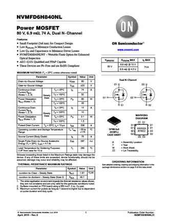
NVMFD6H840NL Power MOSFET 80 V, 6.9 mW, 74 A, Dual N-Channel Features Small Footprint (5x6 mm) for Compact Design Low RDS(on) to Minimize Conduction Losses www.onsemi.com Low QG and Capacitance to Minimize Driver Losses NVMFD6H840NLWF - Wettable Flank Option for Enhanced Optical Inspection V(BR)DSS RDS(ON) MAX ID MAX AEC-Q101 Qualified and PPAP Capable 6.9 mW @ 1... See More ⇒
6.1. Size:190K onsemi
nvmfd6h852nl.pdf 

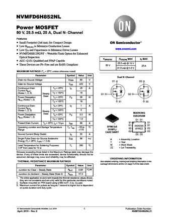
NVMFD6H852NL Power MOSFET 80 V, 25.5 mW, 25 A, Dual N-Channel Features Small Footprint (5x6 mm) for Compact Design Low RDS(on) to Minimize Conduction Losses www.onsemi.com Low QG and Capacitance to Minimize Driver Losses NVMFD6H852NLWF - Wettable Flank Option for Enhanced Optical Inspection V(BR)DSS RDS(ON) MAX ID MAX AEC-Q101 Qualified and PPAP Capable 25.5 mW @... See More ⇒
9.2. Size:229K 1
nvmfd024n06ct1g.pdf 

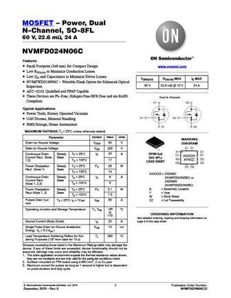
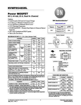
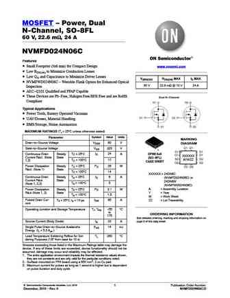
MOSFET Power, Dual N-Channel, SO-8FL 60 V, 22.6 mW, 24 A NVMFD024N06C Features Small Footprint (5x6 mm) for Compact Design www.onsemi.com Low RDS(on) to Minimize Conduction Losses Low QG and Capacitance to Minimize Driver Losses V(BR)DSS RDS(ON) MAX ID MAX NVMFWD024N06C - Wettable Flank Option for Enhanced Optical 60 V 22.6 mW @ 10 V 24 A Inspection AEC-Q101... See More ⇒
9.3. Size:200K 1
nvmfd5483nlt1g.pdf 

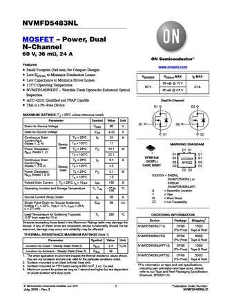
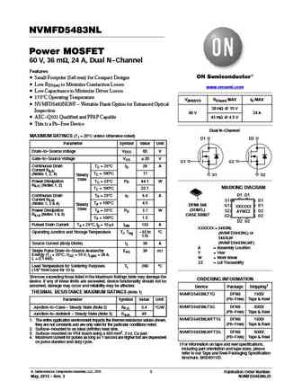
NVMFD5483NL MOSFET Power, Dual N-Channel 60 V, 36 mW, 24 A Features www.onsemi.com Small Footprint (5x6 mm) for Compact Designs Low RDS(on) to Minimize Conduction Losses V(BR)DSS RDS(on) MAX ID MAX Low Capacitance to Minimize Driver Losses 36 mW @ 10 V 175 C Operating Temperature 60 V 24 A NVMFD5483NLWF - Wettable Flank Option for Enhanced Optical 45 mW @ 4... See More ⇒
9.4. Size:206K onsemi
nvmfd5c668nl.pdf 

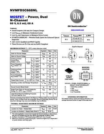
NVMFD5C668NL MOSFET Power, Dual N-Channel 60 V, 6.5 mW, 68 A Features www.onsemi.com Small Footprint (5x6 mm) for Compact Design Low RDS(on) to Minimize Conduction Losses Low QG and Capacitance to Minimize Driver Losses V(BR)DSS RDS(ON) MAX ID MAX NVMFD5C668NLWF - Wettable Flank Option for Enhanced Optical 6.5 mW @ 10 V 60 V Inspection 68 A 9.2 mW @ 4.5 V ... See More ⇒
9.5. Size:209K onsemi
nvmfd5c446nl.pdf 

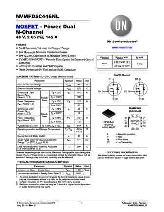
NVMFD5C446NL MOSFET Power, Dual N-Channel 40 V, 2.65 mW, 145 A Features www.onsemi.com Small Footprint (5x6 mm) for Compact Design Low RDS(on) to Minimize Conduction Losses Low QG and Capacitance to Minimize Driver Losses V(BR)DSS RDS(ON) MAX ID MAX NVMFD5C446NLWF - Wettable Flank Option for Enhanced Optical 2.65 mW @ 10 V Inspection 40 V 145 A 3.9 mW @ 4.5 V ... See More ⇒
9.6. Size:203K onsemi
nvmfd5c466n.pdf 

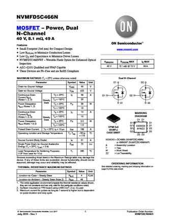
NVMFD5C466N MOSFET Power, Dual N-Channel 40 V, 8.1 mW, 49 A Features Small Footprint (5x6 mm) for Compact Design www.onsemi.com Low RDS(on) to Minimize Conduction Losses Low QG and Capacitance to Minimize Driver Losses NVMFD5C466NWF - Wettable Flank Option for Enhanced Optical V(BR)DSS RDS(ON) MAX ID MAX Inspection 40 V 8.1 mW @ 10 V 49 A AEC-Q101 Qualified ... See More ⇒
9.7. Size:163K onsemi
nvmfd016n06c.pdf 

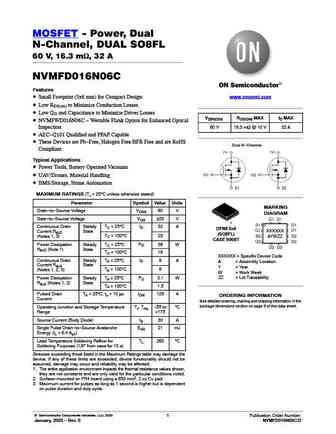
MOSFET - Power, Dual N-Channel, DUAL SO8FL 60 V, 16.3 mW, 32 A NVMFD016N06C Features www.onsemi.com Small Footprint (5x6 mm) for Compact Design Low RDS(on) to Minimize Conduction Losses Low QG and Capacitance to Minimize Driver Losses V(BR)DSS RDS(ON) MAX ID MAX NVMFWD016N06C - Wettable Flank Option for Enhanced Optical Inspection 60 V 16.3 mW @ 10 V 32 A AEC-Q10... See More ⇒
9.8. Size:120K onsemi
nvmfd5853n.pdf 

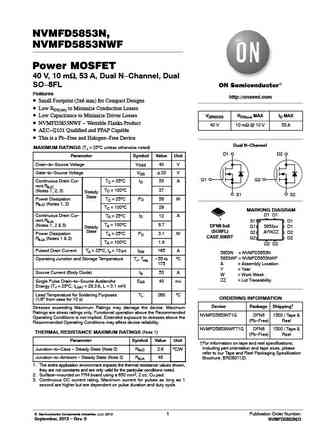
NVMFD5853N, NVMFD5853NWF Power MOSFET 40 V, 10 mW, 53 A, Dual N-Channel, Dual SO-8FL Features http //onsemi.com Small Footprint (5x6 mm) for Compact Designs Low RDS(on) to Minimize Conduction Losses Low Capacitance to Minimize Driver Losses V(BR)DSS RDS(on) MAX ID MAX NVMFD5853NWF - Wettable Flanks Product 40 V 10 mW @ 10 V 53 A AEC-Q101 Qualified and PPAP Capabl... See More ⇒
9.10. Size:268K onsemi
nvmfd5c446n.pdf 

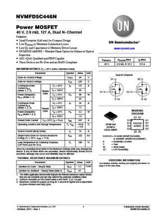
NVMFD5C446N Power MOSFET 40 V, 2.9 mW, 127 A, Dual N-Channel Features Small Footprint (5x6 mm) for Compact Design Low RDS(on) to Minimize Conduction Losses Low QG and Capacitance to Minimize Driver Losses www.onsemi.com NVMFD5C446NWF - Wettable Flank Option for Enhanced Optical Inspection AEC-Q101 Qualified and PPAP Capable V(BR)DSS RDS(ON) MAX ID MAX These D... See More ⇒
9.11. Size:208K onsemi
nvmfd5c650nl.pdf 

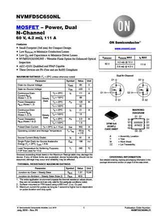
NVMFD5C650NL MOSFET Power, Dual N-Channel 60 V, 4.2 mW, 111 A Features Small Footprint (5x6 mm) for Compact Design www.onsemi.com Low RDS(on) to Minimize Conduction Losses Low QG and Capacitance to Minimize Driver Losses V(BR)DSS RDS(ON) MAX ID MAX NVMFD5C650NLWF - Wettable Flank Option for Enhanced Optical 4.2 mW @ 10 V Inspection 60 V 111 A AEC-Q101 Qual... See More ⇒
9.12. Size:227K onsemi
nvmfd030n06c.pdf 

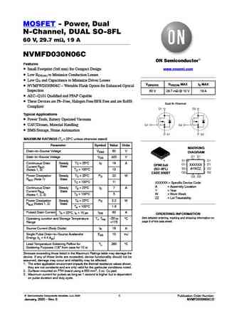
MOSFET - Power, Dual N-Channel, DUAL SO-8FL 60 V, 29.7 mW, 19 A NVMFD030N06C Features www.onsemi.com Small Footprint (5x6 mm) for Compact Design Low RDS(on) to Minimize Conduction Losses Low QG and Capacitance to Minimize Driver Losses V(BR)DSS RDS(ON) MAX ID MAX NVMFWD030N06C - Wettable Flank Option for Enhanced Optical Inspection 60 V 29.7 mW @ 10 V 19 A AEC-Q... See More ⇒
9.13. Size:206K onsemi
nvmfd5c462n.pdf 

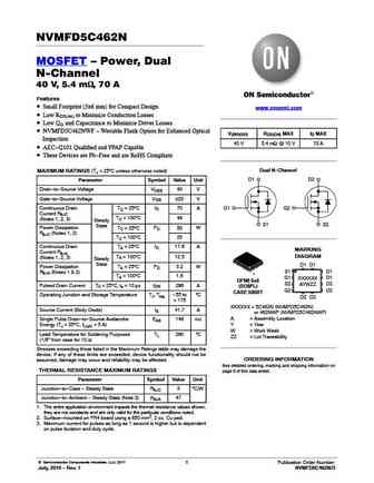
NVMFD5C462N MOSFET Power, Dual N-Channel 40 V, 5.4 mW, 70 A Features Small Footprint (5x6 mm) for Compact Design www.onsemi.com Low RDS(on) to Minimize Conduction Losses Low QG and Capacitance to Minimize Driver Losses NVMFD5C462NWF - Wettable Flank Option for Enhanced Optical V(BR)DSS RDS(ON) MAX ID MAX Inspection 40 V 5.4 mW @ 10 V 70 A AEC-Q101 Qualified ... See More ⇒
9.14. Size:224K onsemi
nvmfd020n06c.pdf 

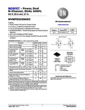
MOSFET - Power, Dual N-Channel, DUAL SO8FL 60 V, 20.3 mW, 27 A NVMFD020N06C Features www.onsemi.com Small Footprint (5x6 mm) for Compact Design Low RDS(on) to Minimize Conduction Losses Low QG and Capacitance to Minimize Driver Losses V(BR)DSS RDS(ON) MAX ID MAX NVMFWD020N06C - Wettable Flank Option for Enhanced Optical Inspection 60 V 20.3 mW @ 10 V 27 A AEC-Q1... See More ⇒
9.16. Size:206K onsemi
nvmfd5c672nl.pdf 

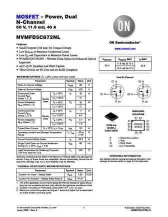
MOSFET Power, Dual N-Channel 60 V, 11.9 mW, 40 A NVMFD5C672NL Features Small Footprint (5x6 mm) for Compact Design www.onsemi.com Low RDS(on) to Minimize Conduction Losses Low QG and Capacitance to Minimize Driver Losses NVMFD5C672NLWF - Wettable Flank Option for Enhanced Optical V(BR)DSS RDS(ON) MAX ID MAX Inspection 11.9 mW @ 10 V 60 V 40 A AEC-Q101 Quali... See More ⇒
9.17. Size:209K onsemi
nvmfd5c470n.pdf 

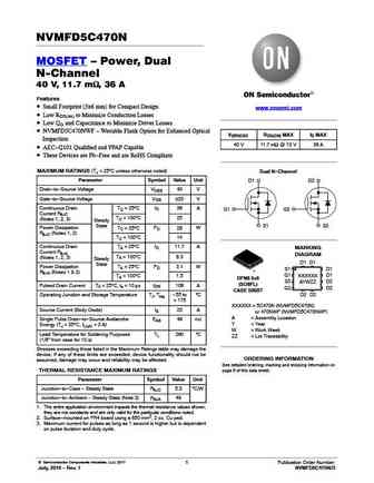
NVMFD5C470N MOSFET Power, Dual N-Channel 40 V, 11.7 mW, 36 A Features Small Footprint (5x6 mm) for Compact Design www.onsemi.com Low RDS(on) to Minimize Conduction Losses Low QG and Capacitance to Minimize Driver Losses NVMFD5C470NWF - Wettable Flank Option for Enhanced Optical V(BR)DSS RDS(ON) MAX ID MAX Inspection 40 V 11.7 mW @ 10 V 36 A AEC-Q101 Qualifie... See More ⇒
9.18. Size:208K onsemi
nvmfd5c466nl.pdf 

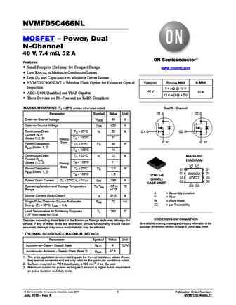
NVMFD5C466NL MOSFET Power, Dual N-Channel 40 V, 7.4 mW, 52 A Features Small Footprint (5x6 mm) for Compact Design www.onsemi.com Low RDS(on) to Minimize Conduction Losses Low QG and Capacitance to Minimize Driver Losses V(BR)DSS RDS(ON) MAX ID MAX NVMFD5C466NLWF - Wettable Flank Option for Enhanced Optical Inspection 7.4 mW @ 10 V 40 V 52 A AEC-Q101 Qualif... See More ⇒
9.19. Size:202K onsemi
nvmfd5853n nvmfd5853nwf.pdf 

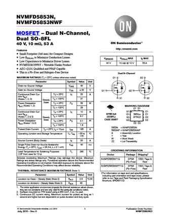
NVMFD5853N, NVMFD5853NWF MOSFET Dual N-Channel, Dual SO-8FL 40 V, 10 mW, 53 A http //onsemi.com Features Small Footprint (5x6 mm) for Compact Designs Low RDS(on) to Minimize Conduction Losses V(BR)DSS RDS(on) MAX ID MAX Low Capacitance to Minimize Driver Losses 40 V 10 mW @ 10 V 53 A NVMFD5853NWF - Wettable Flanks Product AEC-Q101 Qualified and PPAP Capable ... See More ⇒
9.20. Size:78K onsemi
nvmfd5852nl.pdf 

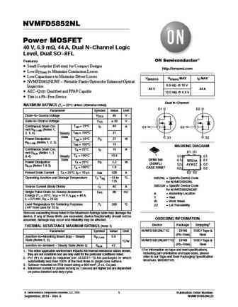
NVMFD5852NL Power MOSFET 40 V, 6.9 mW, 44 A, Dual N-Channel Logic Level, Dual SO-8FL Features Small Footprint (5x6 mm) for Compact Designs http //onsemi.com Low RDS(on) to Minimize Conduction Losses Low Capacitance to Minimize Driver Losses V(BR)DSS RDS(on) MAX ID MAX NVMFD5852NLWF - Wettable Flanks Option for Enhanced Optical 6.9 mW @ 10 V Inspection 40 V 44 A ... See More ⇒
9.21. Size:207K onsemi
nvmfd5c462nl.pdf 

NVMFD5C462NL MOSFET Power, Dual N-Channel 40 V, 4.7 mW, 84 A Features Small Footprint (5x6 mm) for Compact Design www.onsemi.com Low RDS(on) to Minimize Conduction Losses Low QG and Capacitance to Minimize Driver Losses V(BR)DSS RDS(ON) MAX ID MAX NVMFD5C462NLWF - Wettable Flank Option for Enhanced Optical 4.7 mW @ 10 V Inspection 40 V 84 A AEC-Q101 Qualif... See More ⇒
9.22. Size:340K onsemi
nvmfd5c680nl.pdf 

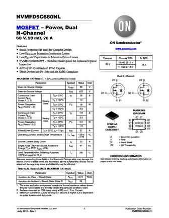
NVMFD5C680NL MOSFET Power, Dual N-Channel 60 V, 28 mW, 26 A Features www.onsemi.com Small Footprint (5x6 mm) for Compact Design Low RDS(on) to Minimize Conduction Losses Low QG and Capacitance to Minimize Driver Losses V(BR)DSS RDS(ON) MAX ID MAX NVMFD5C680NLWF - Wettable Flank Option for Enhanced Optical 28 mW @ 10 V 60 V Inspection 26 A 41 mW @ 4.5 V AE... See More ⇒
9.23. Size:199K onsemi
nvmfd5877nl.pdf 

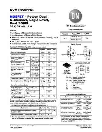
NVMFD5877NL MOSFET Power, Dual N-Channel, Logic Level, Dual SO8FL 60 V, 39 mW, 17 A http //onsemi.com Features Low RDS(on) to Minimize Conduction Losses V(BR)DSS RDS(on) MAX ID MAX Low Capacitance to Minimize Driver Losses 39 mW @ 10 V NVMFD5877NLWF - Wettable Flanks Option for Enhanced Optical 60 V 17 A Inspection 60 mW @ 4.5 V AEC-Q101 Qualified and PPAP Cap... See More ⇒
9.24. Size:76K onsemi
nvmfd5873nl.pdf 

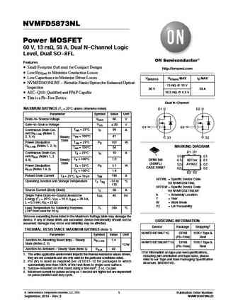
NVMFD5873NL Power MOSFET 60 V, 13 mW, 58 A, Dual N-Channel Logic Level, Dual SO-8FL Features Small Footprint (5x6 mm) for Compact Designs http //onsemi.com Low RDS(on) to Minimize Conduction Losses Low Capacitance to Minimize Driver Losses V(BR)DSS RDS(on) MAX ID MAX NVMFD5873NLWF - Wettable Flanks Option for Enhanced Optical 13 mW @ 10 V Inspection 60 V 58 A 16.5 ... See More ⇒
9.25. Size:75K onsemi
nvmfd5853nl.pdf 

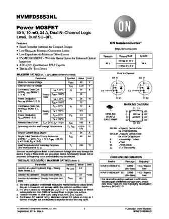
NVMFD5853NL Power MOSFET 40 V, 10 mW, 34 A, Dual N-Channel Logic Level, Dual SO-8FL Features Small Footprint (5x6 mm) for Compact Designs http //onsemi.com Low RDS(on) to Minimize Conduction Losses Low Capacitance to Minimize Driver Losses V(BR)DSS RDS(on) MAX ID MAX NVMFD5853NLWF - Wettable Flanks Option for Enhanced Optical 10 mW @ 10 V Inspection 40 V 34 A A... See More ⇒
9.26. Size:196K onsemi
nvmfd5c478n.pdf 

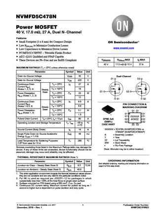
NVMFD5C478N Power MOSFET 40 V, 17.0 mW, 27 A, Dual N-Channel Features Small Footprint (5 x 6 mm) for Compact Design Low RDS(on) to Minimize Conduction Losses www.onsemi.com Low Capacitance to Minimize Driver Losses NVMFD5C478NWF - Wettable Flanks Product AEC-Q101 Qualified and PPAP Capable V(BR)DSS RDS(on) MAX ID MAX These Devices are Pb-Free and are RoHS Comp... See More ⇒
9.27. Size:229K onsemi
nvmfd024n06c.pdf 

MOSFET Power, Dual N-Channel, SO-8FL 60 V, 22.6 mW, 24 A NVMFD024N06C Features Small Footprint (5x6 mm) for Compact Design www.onsemi.com Low RDS(on) to Minimize Conduction Losses Low QG and Capacitance to Minimize Driver Losses V(BR)DSS RDS(ON) MAX ID MAX NVMFWD024N06C - Wettable Flank Option for Enhanced Optical 60 V 22.6 mW @ 10 V 24 A Inspection AEC-Q101... See More ⇒
9.28. Size:347K onsemi
nvmfd5c674nl.pdf 

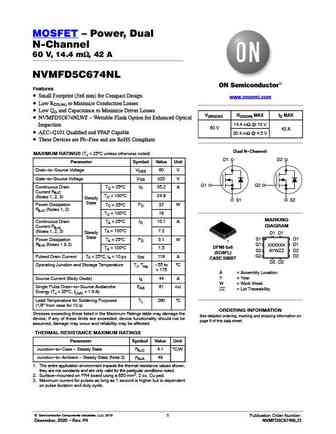
MOSFET Power, Dual N-Channel 60 V, 14.4 mW, 42 A NVMFD5C674NL Features Small Footprint (5x6 mm) for Compact Design www.onsemi.com Low RDS(on) to Minimize Conduction Losses Low QG and Capacitance to Minimize Driver Losses V(BR)DSS RDS(ON) MAX ID MAX NVMFD5C674NLWF - Wettable Flank Option for Enhanced Optical 14.4 mW @ 10 V Inspection 60 V 42 A AEC-Q101 Qual... See More ⇒
9.29. Size:201K onsemi
nvmfd5875nl.pdf 

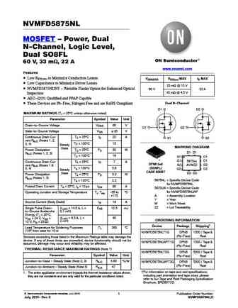
NVMFD5875NL MOSFET Power, Dual N-Channel, Logic Level, Dual SO8FL 60 V, 33 mW, 22 A www.onsemi.com Features Low RDS(on) to Minimize Conduction Losses V(BR)DSS RDS(on) MAX ID MAX Low Capacitance to Minimize Driver Losses 33 mW @ 10 V NVMFD5875NLWF - Wettable Flanks Option for Enhanced Optical 60 V 22 A 45 mW @ 4.5 V Inspection AEC-Q101 Qualified and PPAP Capabl... See More ⇒
9.30. Size:77K onsemi
nvmfd5489nl.pdf 

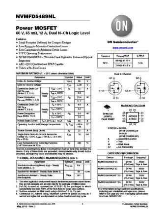
NVMFD5489NL Power MOSFET 60 V, 65 mW, 12 A, Dual N-Ch Logic Level Features Small Footprint (5x6 mm) for Compact Designs Low RDS(on) to Minimize Conduction Losses www.onsemi.com Low Capacitance to Minimize Driver Losses 175 C Operating Temperature V(BR)DSS RDS(on) MAX ID MAX NVMFD5489NLWF - Wettable Flank Option for Enhanced Optical 65 mW @ 10 V Inspection 60 V ... See More ⇒
9.31. Size:200K onsemi
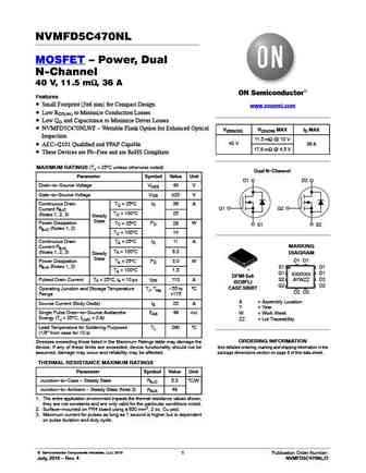
nvmfd5c470nl.pdf 

NVMFD5C470NL MOSFET Power, Dual N-Channel 40 V, 11.5 mW, 36 A Features Small Footprint (5x6 mm) for Compact Design www.onsemi.com Low RDS(on) to Minimize Conduction Losses Low QG and Capacitance to Minimize Driver Losses NVMFD5C470NLWF - Wettable Flank Option for Enhanced Optical V(BR)DSS RDS(ON) MAX ID MAX Inspection 11.5 mW @ 10 V 40 V AEC-Q101 Qualified ... See More ⇒
9.32. Size:155K onsemi
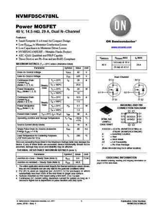
nvmfd5c478nl.pdf 

NVMFD5C478NL Power MOSFET 40 V, 14.5 mW, 29 A, Dual N-Channel Features Small Footprint (5 x 6 mm) for Compact Design Low RDS(on) to Minimize Conduction Losses www.onsemi.com Low Capacitance to Minimize Driver Losses NVMFD5C478NLWF - Wettable Flanks Product AEC-Q101 Qualified and PPAP Capable V(BR)DSS RDS(on) MAX ID MAX These Devices are Pb-Free and are RoHS Co... See More ⇒
Detailed specifications: NVMFD5C478N, NVMFD5C478NL, NVMFD5C650NL, NVMFD5C668NL, NVMFD5C672NL, NVMFD5C674NL, NVMFD5C680NL, NVMFD6H840NL, IRF640N, NVMFD6H852NL, NVMFS015N10MCL, NVMFS016N06C, NVMFS020N06C, NVMFS024N06C, NVMFS3D6N10MCL, NVMFS4C302N, NVMFS4C310N
Keywords - NVMFD6H846NL MOSFET specs
NVMFD6H846NL cross reference
NVMFD6H846NL equivalent finder
NVMFD6H846NL pdf lookup
NVMFD6H846NL substitution
NVMFD6H846NL replacement
Can't find your MOSFET?
Learn how to find a substitute transistor by analyzing voltage, current and package compatibility
