NVMFS6H852N Specs and Replacement
Type Designator: NVMFS6H852N
Type of Transistor: MOSFET
Type of Control Channel: N-Channel
Absolute Maximum Ratings
Pd ⓘ - Maximum Power Dissipation: 54 W
|Vds|ⓘ - Maximum Drain-Source Voltage: 80 V
|Vgs|ⓘ - Maximum Gate-Source Voltage: 20 V
|Id| ⓘ - Maximum Drain Current: 40 A
Tj ⓘ - Maximum Junction Temperature: 175 °C
Electrical Characteristics
tr ⓘ - Rise Time: 24 nS
Cossⓘ - Output Capacitance: 110 pF
RDSonⓘ - Maximum Drain-Source On-State Resistance: 0.0142 Ohm
Package: DFN5
NVMFS6H852N substitution
- MOSFET ⓘ Cross-Reference Search
NVMFS6H852N datasheet
nvmfs6h852n.pdf
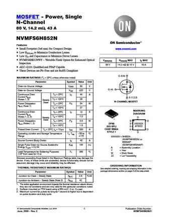
MOSFET - Power, Single N-Channel 80 V, 14.2 mW, 43 A NVMFS6H852N Features www.onsemi.com Small Footprint (5x6 mm) for Compact Design Low RDS(on) to Minimize Conduction Losses Low QG and Capacitance to Minimize Driver Losses NVMFS6H852NWF - Wettable Flank Option for Enhanced Optical V(BR)DSS RDS(ON) MAX ID MAX Inspection 80 V 14.2 mW @ 10 V 43 A AEC-Q101 Qualifie... See More ⇒
nvmfs6h852nl.pdf
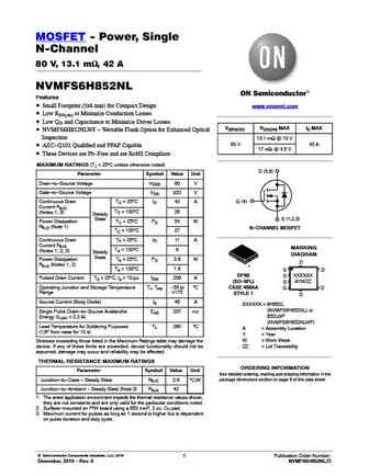
MOSFET - Power, Single N-Channel 80 V, 13.1 mW, 42 A NVMFS6H852NL Features Small Footprint (5x6 mm) for Compact Design www.onsemi.com Low RDS(on) to Minimize Conduction Losses Low QG and Capacitance to Minimize Driver Losses V(BR)DSS RDS(ON) MAX ID MAX NVMFS6H852NLWF - Wettable Flank Option for Enhanced Optical Inspection 13.1 mW @ 10 V 80 V 42 A AEC-Q101 Quali... See More ⇒
nvmfs6h858nl.pdf
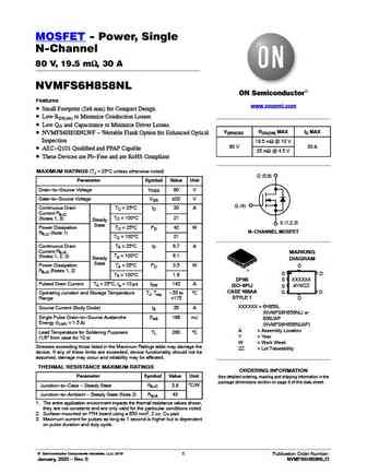
MOSFET - Power, Single N-Channel 80 V, 19.5 mW, 30 A NVMFS6H858NL Features www.onsemi.com Small Footprint (5x6 mm) for Compact Design Low RDS(on) to Minimize Conduction Losses Low QG and Capacitance to Minimize Driver Losses V(BR)DSS RDS(ON) MAX ID MAX NVMFS6H858NLWF - Wettable Flank Option for Enhanced Optical Inspection 19.5 mW @ 10 V 80 V 30 A AEC-Q101 Quali... See More ⇒
nvmfs6h858n.pdf

MOSFET - Power, Single N-Channel 80 V, 20.7 mW, 32 A NVMFS6H858N Features www.onsemi.com Small Footprint (5x6 mm) for Compact Design Low RDS(on) to Minimize Conduction Losses Low QG and Capacitance to Minimize Driver Losses NVMFS6H858NWF - Wettable Flank Option for Enhanced Optical V(BR)DSS RDS(ON) MAX ID MAX Inspection 80 V 20.7 mW @ 10 V 32 A AEC-Q101 Qualifie... See More ⇒
Detailed specifications: NVMFS6H818N, NVMFS6H818NL, NVMFS6H824N, NVMFS6H824NL, NVMFS6H836N, NVMFS6H836NL, NVMFS6H848N, NVMFS6H848NL, IRF520, NVMFS6H852NL, NVMFS6H858N, NVMFS6H858NL, NVMFS6H864N, NVMFS6H864NL, NVMTS0D4N04CL, NVMTS0D6N04C, NVMTS0D7N04C
Keywords - NVMFS6H852N MOSFET specs
NVMFS6H852N cross reference
NVMFS6H852N equivalent finder
NVMFS6H852N pdf lookup
NVMFS6H852N substitution
NVMFS6H852N replacement
Can't find your MOSFET? Learn how to find a substitute transistor by analyzing voltage, current and package compatibility
🌐 : EN ES РУ

LIST
Last Update
MOSFET: FTF30P35D | FTF25N35DHVT | FTF15N35D | FTE15C35G | FTP02P15G | FTE02P15G | AKF30N5P0SX | AKF30N10S | AKF20P45D | CM4407
Popular searches
ksa1381 replacement | m3056m mosfet | skd502t mosfet | tip 35 transistor | bu2508df | 2n2222a transistor equivalent | 2sc2509 | 2n1815