PJM2302NSA-S Specs and Replacement
Type Designator: PJM2302NSA-S
Type of Transistor: MOSFET
Type of Control Channel: N-Channel
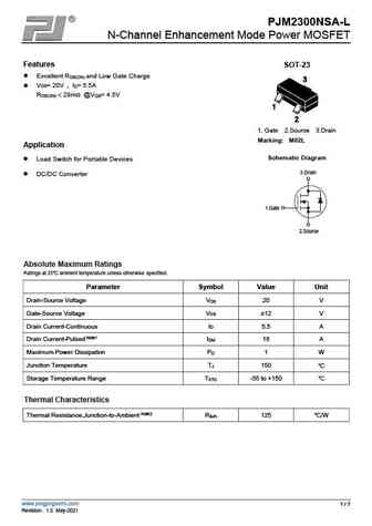
Absolute Maximum Ratings
Pd ⓘ - Maximum Power Dissipation: 0.9 W
|Vds|ⓘ - Maximum Drain-Source Voltage: 20 V
|Vgs|ⓘ - Maximum Gate-Source Voltage: 12 V
|Id| ⓘ - Maximum Drain Current: 2 A
Tj ⓘ - Maximum Junction Temperature: 150 °C
Electrical Characteristics
tr ⓘ - Rise Time: 3.2 nS
Cossⓘ - Output Capacitance: 48 pF
RDSonⓘ - Maximum Drain-Source On-State Resistance: 0.05 Ohm
Package: SOT23
PJM2302NSA-S substitution
- MOSFET ⓘ Cross-Reference Search
PJM2302NSA-S datasheet
pjm2302nsa-s.pdf
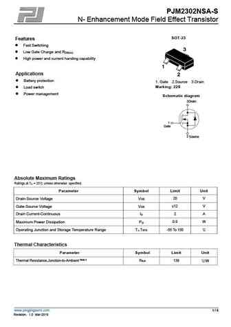
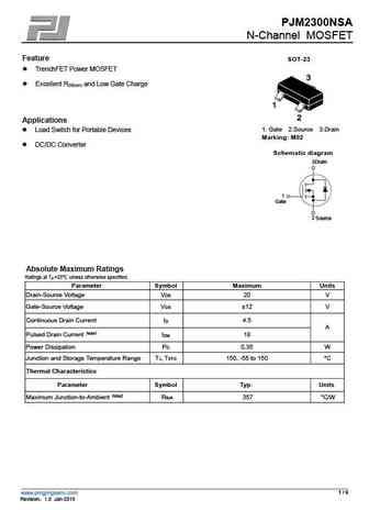
PJM2302NSA-S N- Enhancement Mode Field Effect Transistor SOT-23 Features Fast Switching Low Gate Charge and R DS(on) High power and current handing capability Applications Battery protection 1. Gate 2.Source 3.Drain Marking 22S Load switch Power management Schematic diagram 3Drain 1 Gate 2 Source Absolute Maximum Ratings Ratings at TC = 25 unle... See More ⇒
pjm2302nsa.pdf
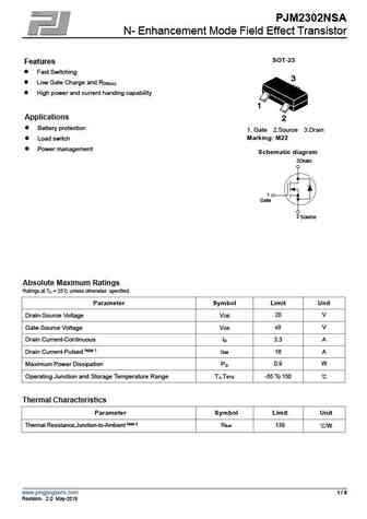
PJM2302NSA N- Enhancement Mode Field Effect Transistor SOT-23 Features Fast Switching Low Gate Charge and R DS(on) High power and current handing capability Applications Battery protection 1. Gate 2.Source 3.Drain Marking M22 Load switch Power management Schematic diagram 3Drain 1 Gate 2 Source Absolute Maximum Ratings Ratings at TC = 25 unless... See More ⇒
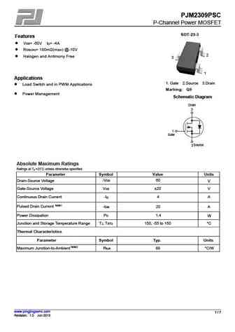
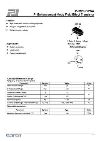
pjm2301psa-s.pdf
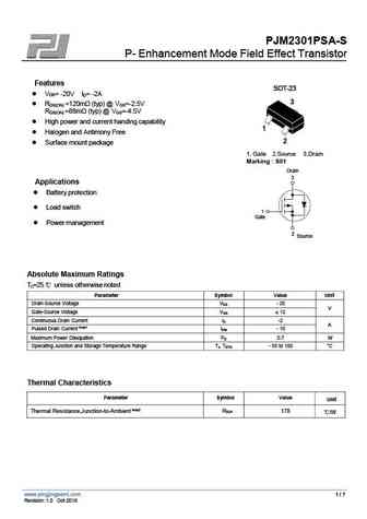
PJM2301PSA-S P- Enhancement Mode Field Effect Transistor Features SOT-23 VDS= -20V I = -2A D R =120m (typ) @ V =-2.5V DS(ON) GS R =88m (typ) @ V =-4.5V DS(ON) GS High power and current handing capability Halogen and Antimony Free Surface mount package 1. Gate 2.Source 3.Drain Marking S01 Drain 3 Applications Battery protection Load s... See More ⇒
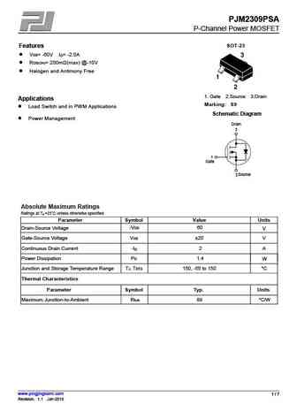
pjm2305psa.pdf
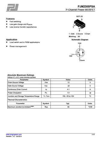
PJM2305PSA P-Channel Power MOSFET SOT-23 Features Fast switching Low gate charge and R DS(ON) Low reverse transfer capacitances 1. Gate 2.Source 3.Drain Marking S5 Application Schematic Diagram Load switch and in PWM applicatopns Drain 3 Power management 1 Gate Source 2 Absolute Maximum Ratings Ratings at TA =25 unless otherwise specified. Paramete... See More ⇒
Detailed specifications: PJM07P20SA, PJM10H03NSC, PJM138NSA, PJM2300NSA, PJM2300NSA-L, PJM2301PSA, PJM2301PSA-S, PJM2302NSA, IRF9540, PJM2305PSA, PJM2309PSA, PJM2309PSC, PJM2319PSA, PJM3400NSA, PJM3400NSC, PJM3401PSA, PJM3401PSC
Keywords - PJM2302NSA-S MOSFET specs
PJM2302NSA-S cross reference
PJM2302NSA-S equivalent finder
PJM2302NSA-S pdf lookup
PJM2302NSA-S substitution
PJM2302NSA-S replacement
Learn how to find the right MOSFET substitute. A guide to cross-reference, check specs and replace MOSFETs in your circuits.
History: SI9410BDY-T1
🌐 : EN ES РУ

LIST
Last Update
MOSFET: AUB034N10 | AUB033N08BG | AUB026N085 | AUA062N08BG | AUA060N08AG | AUA056N08BGL | AUA039N10 | ASW80R290E | ASW65R120EFD | ASW65R110E
Popular searches
irf640 | irf840 | irf740 | c945 transistor | irf640n | 2n3904 | bc547 datasheet | k3797 mosfet