PNMT6N1-LB Specs and Replacement
Type Designator: PNMT6N1-LB
Type of Transistor: MOSFET
Type of Control Channel: N-Channel
Absolute Maximum Ratings
Pd ⓘ - Maximum Power Dissipation: 0.15 W
|Vds|ⓘ - Maximum Drain-Source Voltage: 40 V
|Vgs|ⓘ - Maximum Gate-Source Voltage: 20 V
|Id| ⓘ - Maximum Drain Current: 0.18 A
Tj ⓘ - Maximum Junction Temperature: 150 °C
Electrical Characteristics
Cossⓘ - Output Capacitance: 20 max pF
RDSonⓘ - Maximum Drain-Source On-State Resistance: 4 Ohm
Package: DFN2X2-6L
PNMT6N1-LB substitution
- MOSFET ⓘ Cross-Reference Search
PNMT6N1-LB datasheet
pnmt6n1-lb.pdf
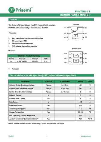
PNMT6N1-LB Transistor with N-MOSFET Feature Top View This device is Pb-Free, Halogen Free/BFR Free and RoHS compliant. E 1 PNMT6N1-LB is composed by a transistor and a MOSFET 6 C Transistor B 2 G 5 S D 3 4 Very low collector to emitter saturation voltage DC current gain ... See More ⇒
pnmt6n1.pdf
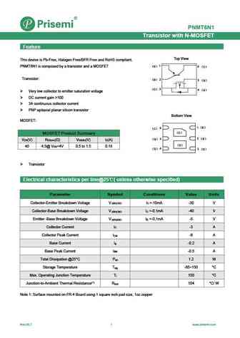
PNMT6N1 Transistor with N-MOSFET Feature Top View This device is Pb-Free, Halogen Free/BFR Free and RoHS compliant. 1 PNMT6N1 is composed by a transistor and a MOSFET 6 E C Transistor 2 B 5 G 3 D 4 S Very low collector to emitter saturation voltage DC current gain >100 3A continuous collector current PNP epitaxial planar ... See More ⇒
pnmt6n2.pdf
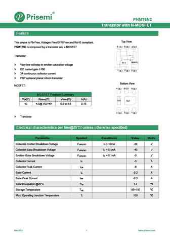
PNMT6N2 Transistor with N-MOSFET Feature Top View This device is Pb-Free, Halogen Free/BFR Free and RoHS compliant. 6 5 C 4 PNMT6N2 is composed by a transistor and a MOSFET C S Transistor 8(B/D) 7(C) Very low collector to emitter saturation voltage DC current gain >100 1 2 3 E E G 3A continuous collector current PNP epitaxial... See More ⇒
pnmt60v02.pdf
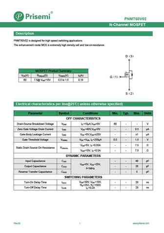
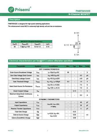
PNMT60V02 N-Channel MOSFET Description PNMT60V02 is designed for high speed switching applications The enhancement mode MOS is extremely high density cell and low on-resistance. D 3 MOSFET Product Summary VDS(V) RDS(on)( ) VGS(th)(V) ID(A) G 1 60 7.5@ VGS=10V 0.5 to 1.5 0.18 S 2 Electrical characteristics per line@25 ( unless otherwise specified) Par... See More ⇒
Detailed specifications: SC8205, SC8205S, PDNM6ET20V05, PNM3FD201E0, PNM3FD20V1E, PNM523T30V01, PNM723T30V01, PNMT6N1, IRFB7545, PNMT6N2, PNMT8N1, PPMT2301, PJ2301-AU, PJA3415AE, PJA3416AE, PJA3417, PJA3419
Keywords - PNMT6N1-LB MOSFET specs
PNMT6N1-LB cross reference
PNMT6N1-LB equivalent finder
PNMT6N1-LB pdf lookup
PNMT6N1-LB substitution
PNMT6N1-LB replacement
Learn how to find the right MOSFET substitute. A guide to cross-reference, check specs and replace MOSFETs in your circuits.
History: IRLU2905ZPBF
🌐 : EN ES РУ
LIST
Last Update
MOSFET: AUB034N10 | AUB033N08BG | AUB026N085 | AUA062N08BG | AUA060N08AG | AUA056N08BGL | AUA039N10 | ASW80R290E | ASW65R120EFD | ASW65R110E
Popular searches
c2078 transistor | 2sc458 transistors | 2sa992 | 2sa970 | a970 | d2390 transistor | 2n5087 equivalent | tip147 datasheet
