PTF10HN08 Datasheet. Specs and Replacement
Type Designator: PTF10HN08 📄📄
Type of Transistor: MOSFET
Type of Control Channel: N-Channel
Absolute Maximum Ratings
Pd ⓘ - Maximum Power Dissipation: 200 W
|Vds|ⓘ - Maximum Drain-Source Voltage: 80 V
|Vgs|ⓘ - Maximum Gate-Source Voltage: 25 V
|Id| ⓘ - Maximum Drain Current: 100 A
Tj ⓘ - Maximum Junction Temperature: 175 °C
Electrical Characteristics
tr ⓘ - Rise Time: 64 nS
Cossⓘ - Output Capacitance: 440 pF
RDSonⓘ - Maximum Drain-Source On-State Resistance: 0.0085 Ohm
Package: TO220F
📄📄 Copy
PTF10HN08 substitution
- MOSFET ⓘ Cross-Reference Search
PTF10HN08 datasheet
ptf10hn08 pty10hn08.pdf
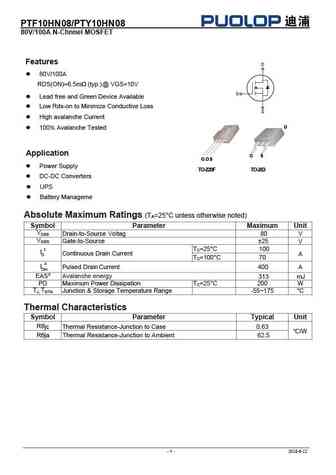
PTF10HN08/PTY10HN08 80V/100A N-Chnnel MOSFET Features D 80V/100A RDS(ON)=6.5m (typ.)@ VGS=10V G Lead free and Green Device Available Low Rds-on to Minimize Conductive Loss S High avalanche Current D % 100 Avalanche Tested Application G S G D S Power Supply TO-220F TO-263 DC-DC Converters UPS Battery Manageme e Absolute Maximum Ratings... See More ⇒
ptf10149.pdf
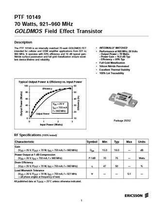
PTF 10149 70 Watts, 921 960 MHz GOLDMOS Field Effect Transistor Description INTERNALLY MATCHED The PTF 10149 is an internally matched 70 watt GOLDMOS FET intended for cellular and GSM amplifier applications from 921 to Performance at 960 MHz, 26 Volts 960 MHz. It operates with 50% efficiency and 16 dB typical gain. - Output Power = 70 Watts Nitride surface passivation and ... See More ⇒
ptf10n65.pdf
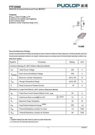
PTF1 0N65 65 0V/1 0A N-Channel A dv anced Power MOSFET Features RDS(on) (Typical 0.6 )@VGS=10V Improved dv/dt Capability, High Ruggedness 100% Avalanche Tested Maximum Junction Temperature Range (150 C) G D S TO-220F Absolute Maximum Ratings Stresses exceeding Maximum Ratings may damage the device. Maximum Ratings are stress ratings only. Functional operation above... See More ⇒
Detailed specifications: PTD3006, PTD4080B, PTD4N60, PTD50N06, PTD60N02, PTD7N65, PTD80N06, PTF10N65, 2SK3878, PTY10HN08, PTF12N65, PTF13N50, PTF2N65, PTF5N65, PTF7N65, PTF8N65, PTN3006
Keywords - PTF10HN08 MOSFET specs
PTF10HN08 cross reference
PTF10HN08 equivalent finder
PTF10HN08 pdf lookup
PTF10HN08 substitution
PTF10HN08 replacement
Can't find your MOSFET? Learn how to find a substitute transistor by analyzing voltage, current and package compatibility
