SE10080A Specs and Replacement
Type Designator: SE10080A
Type of Transistor: MOSFET
Type of Control Channel: N-Channel
Absolute Maximum Ratings
Pd ⓘ
- Maximum Power Dissipation: 200 W
|Vds|ⓘ - Maximum Drain-Source Voltage: 100 V
|Vgs|ⓘ - Maximum Gate-Source Voltage: 20 V
|Id| ⓘ - Maximum Drain Current: 80 A
Tj ⓘ - Maximum Junction Temperature: 175 °C
Electrical Characteristics
tr ⓘ - Rise Time: 50 nS
Cossⓘ -
Output Capacitance: 340 pF
RDSonⓘ - Maximum Drain-Source On-State Resistance: 0.013 Ohm
Package: TO220
- MOSFET ⓘ Cross-Reference Search
SE10080A datasheet
..1. Size:624K cn sino-ic
se10080a.pdf 
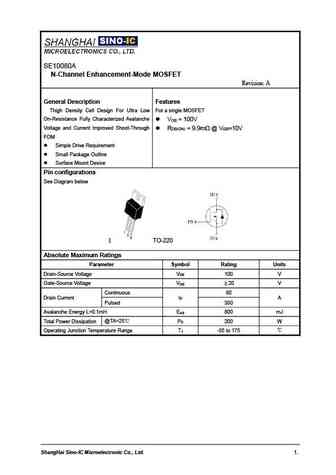
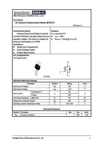
SE10080A N-Channel Enhancement-Mode MOSFET Revision A General Description Features Thigh Density Cell Design For Ultra Low For a single MOSFET On-Resistance Fully Characterized Avalanche V =100V DS Voltage and Current Improved Shoot-Through R =9.9m @V =10V DS(ON) GS FOM Simple Drive Requirement Small Package Outline Surface Mount Device Pin configurations ... See More ⇒
9.1. Size:358K cn sino-ic
se100p60.pdf
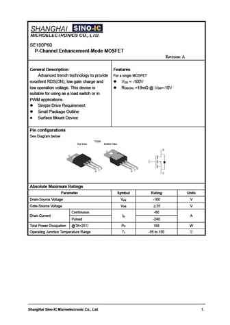
SE100P60 P-Channel Enhancement-Mode MOSFET Revision A General Description Features For a single MOSFET Advanced trench technology to provide excellent RDS(ON), low gate charge and V = -100V DS low operation voltage. This device is R =18m @V =-10V DS(ON) GS suitable for using as a load switch or in PWM applications. Simple Drive Requirement Small Package Outline ... See More ⇒
9.3. Size:470K cn sino-ic
se100150g.pdf
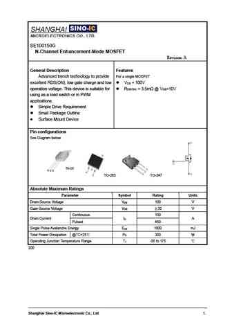
SE100150G N-Channel Enhancement-Mode MOSFET Revision A General Description Features For a single MOSFET Advanced trench technology to provide excellent RDS(ON), low gate charge and low V =100V DS operation voltage. This device is suitable for R =3.5m @V =10V DS(ON) GS using as a load switch or in PWM applications. Simple Drive Requirement Small Package Outline ... See More ⇒
9.4. Size:399K cn sino-ic
se10015.pdf
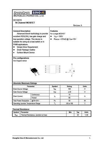
SE10015 N-Channel MOSFET Revision A General Description Features For a single MOSFET Advanced trench technology to provide excellent RDS(ON), low gate charge and V =100V DS low operation voltage. This device is R =67m @V =10V DS(ON) GS suitable for using as a load switch or in PWM applications. Simple Drive Requirement Small Package Outline Surface Mount De... See More ⇒
9.5. Size:289K cn sino-ic
se100130ga.pdf
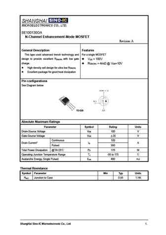
SE100130GA N-Channel Enhancement-Mode MOSFET Revision A General Description Features This type used advanced trench technology and For a single MOSFET design to provide excellent R with low gate DS(ON) V =100V DS charge. R =4m @V =10V DS(ON) GS High density cell design for ultra low R DS(ON) Excellent package for good heat dissipation Pin configurations See Di... See More ⇒
9.6. Size:576K cn sino-ic
se1003.pdf
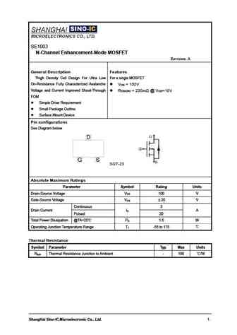
SE1003 N-Channel Enhancement-Mode MOSFET Revision A General Description Features Thigh Density Cell Design For Ultra Low For a single MOSFET On-Resistance Fully Characterized Avalanche V = 100V DS Voltage and Current Improved Shoot-Through R = 230m @ V =10V DS(ON) GS FOM Simple Drive Requirement Small Package Outline Surface Mount Device Pin configurations ... See More ⇒
9.7. Size:418K cn sino-ic
se100130a.pdf
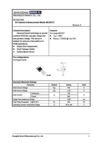
SE100130A N-Channel Enhancement-Mode MOSFET Revision A General Description Features For a single MOSFET Advanced trench technology to provide excellent RDS(ON), low gate charge and V = 100V DS low operation voltage. This device is R =3.0m @V =10V DS(ON) GS suitable for using as a load switch or in PWM applications. Simple Drive Requirement Small Package Outline ... See More ⇒
9.8. Size:290K cn sino-ic
se100180ga.pdf
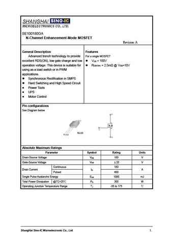
SE100180GA N-Channel Enhancement-Mode MOSFET Revision A General Description Features For a single MOSFET Advanced trench technology to provide excellent RDS(ON), low gate charge and low V =100V DS operation voltage. This device is suitable for R =2.5m @V =10V DS(ON) GS using as a load switch or in PWM applications. Synchronous Rectification in SMPS Hard Switchin... See More ⇒
9.9. Size:338K cn sino-ic
se100250gts.pdf
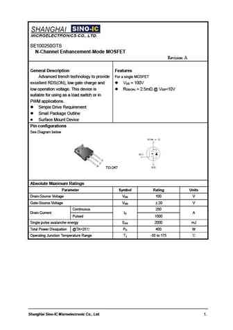
SE100250GTS N-Channel Enhancement-Mode MOSFET Revision A General Description Features For a single MOSFET Advanced trench technology to provide excellent RDS(ON), low gate charge and V = 100V DS low operation voltage. This device is R =2.5m @V =10V DS(ON) GS suitable for using as a load switch or in PWM applications. Simple Drive Requirement Small Package Outlin... See More ⇒
9.10. Size:420K cn sino-ic
se10030a.pdf
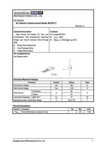
SE10030A N-Channel Enhancement-Mode MOSFET Revision A General Description Features Thigh Density Cell Design For Ultra Low For a single MOSFET On-Resistance Fully Characterized Avalanche V =100V DS Voltage and Current Improved Shoot-Through R =25m @V =10V DS(ON) GS FOM Simple Drive Requirement Small Package Outline Surface Mount Device Pin configurations ... See More ⇒
Detailed specifications: SE100130GA, SE10015, SE100150G, SE100180GA, SE100250GTS, SE1003, SE10030A, SE10060A, CS150N03A8, SE100P60, SE120120G, SE12060GA, SE1216, SE12N50FRA, SE12N65, SE138U, SE150110G
Keywords - SE10080A MOSFET specs
SE10080A cross reference
SE10080A equivalent finder
SE10080A pdf lookup
SE10080A substitution
SE10080A replacement
Step-by-step guide to finding a MOSFET replacement. Cross-reference parts and ensure compatibility for your repair or project.