SE10080A datasheet, аналоги, основные параметры
Наименование производителя: SE10080A 📄📄
Тип транзистора: MOSFET
Полярность: N
Предельные значения
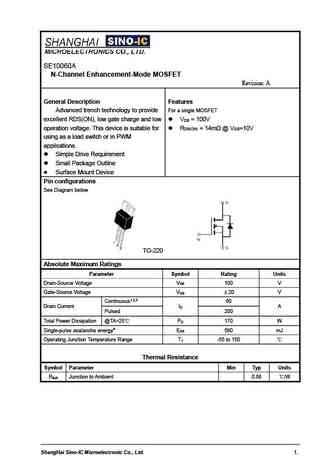
Pd ⓘ - Максимальная рассеиваемая мощность: 200 W
|Vds|ⓘ - Максимально допустимое напряжение сток-исток: 100 V
|Vgs|ⓘ - Максимально допустимое напряжение затвор-исток: 20 V
|Id| ⓘ - Максимально допустимый постоянный ток стока: 80 A
Tj ⓘ - Максимальная температура канала: 175 °C
Электрические характеристики
tr ⓘ - Время нарастания: 50 ns
Cossⓘ - Выходная емкость: 340 pf
RDSonⓘ - Сопротивление сток-исток открытого транзистора: 0.013 Ohm
Тип корпуса: TO220
📄📄 Копировать
Аналог (замена) для SE10080A
- подборⓘ MOSFET транзистора по параметрам
SE10080A даташит
..1. Size:624K cn sino-ic
se10080a.pdf 
SE10080A N-Channel Enhancement-Mode MOSFET Revision A General Description Features Thigh Density Cell Design For Ultra Low For a single MOSFET On-Resistance Fully Characterized Avalanche V =100V DS Voltage and Current Improved Shoot-Through R =9.9m @V =10V DS(ON) GS FOM Simple Drive Requirement Small Package Outline Surface Mount Device Pin configurations
9.1. Size:358K cn sino-ic
se100p60.pdf 
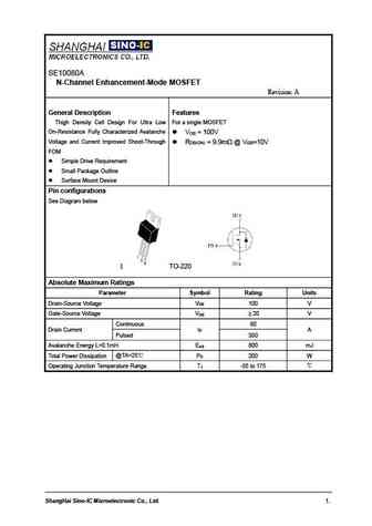
SE100P60 P-Channel Enhancement-Mode MOSFET Revision A General Description Features For a single MOSFET Advanced trench technology to provide excellent RDS(ON), low gate charge and V = -100V DS low operation voltage. This device is R =18m @V =-10V DS(ON) GS suitable for using as a load switch or in PWM applications. Simple Drive Requirement Small Package Outline
9.3. Size:470K cn sino-ic
se100150g.pdf 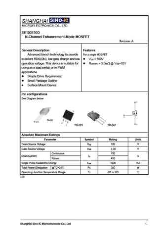
SE100150G N-Channel Enhancement-Mode MOSFET Revision A General Description Features For a single MOSFET Advanced trench technology to provide excellent RDS(ON), low gate charge and low V =100V DS operation voltage. This device is suitable for R =3.5m @V =10V DS(ON) GS using as a load switch or in PWM applications. Simple Drive Requirement Small Package Outline
9.4. Size:399K cn sino-ic
se10015.pdf 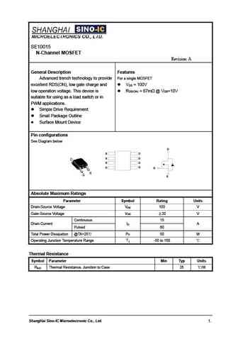
SE10015 N-Channel MOSFET Revision A General Description Features For a single MOSFET Advanced trench technology to provide excellent RDS(ON), low gate charge and V =100V DS low operation voltage. This device is R =67m @V =10V DS(ON) GS suitable for using as a load switch or in PWM applications. Simple Drive Requirement Small Package Outline Surface Mount De
9.5. Size:289K cn sino-ic
se100130ga.pdf 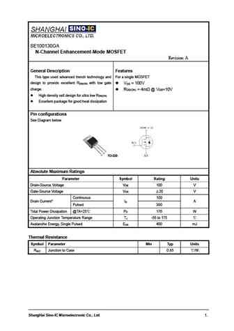
SE100130GA N-Channel Enhancement-Mode MOSFET Revision A General Description Features This type used advanced trench technology and For a single MOSFET design to provide excellent R with low gate DS(ON) V =100V DS charge. R =4m @V =10V DS(ON) GS High density cell design for ultra low R DS(ON) Excellent package for good heat dissipation Pin configurations See Di
9.6. Size:576K cn sino-ic
se1003.pdf 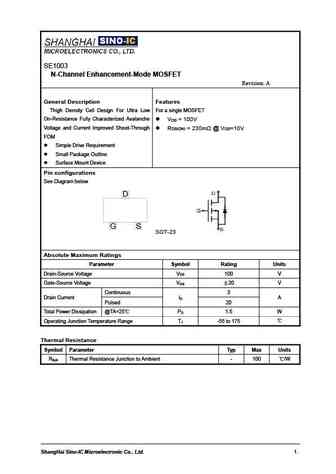
SE1003 N-Channel Enhancement-Mode MOSFET Revision A General Description Features Thigh Density Cell Design For Ultra Low For a single MOSFET On-Resistance Fully Characterized Avalanche V = 100V DS Voltage and Current Improved Shoot-Through R = 230m @ V =10V DS(ON) GS FOM Simple Drive Requirement Small Package Outline Surface Mount Device Pin configurations
9.7. Size:418K cn sino-ic
se100130a.pdf 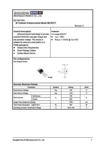
SE100130A N-Channel Enhancement-Mode MOSFET Revision A General Description Features For a single MOSFET Advanced trench technology to provide excellent RDS(ON), low gate charge and V = 100V DS low operation voltage. This device is R =3.0m @V =10V DS(ON) GS suitable for using as a load switch or in PWM applications. Simple Drive Requirement Small Package Outline
9.8. Size:290K cn sino-ic
se100180ga.pdf 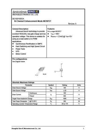
SE100180GA N-Channel Enhancement-Mode MOSFET Revision A General Description Features For a single MOSFET Advanced trench technology to provide excellent RDS(ON), low gate charge and low V =100V DS operation voltage. This device is suitable for R =2.5m @V =10V DS(ON) GS using as a load switch or in PWM applications. Synchronous Rectification in SMPS Hard Switchin
9.9. Size:338K cn sino-ic
se100250gts.pdf 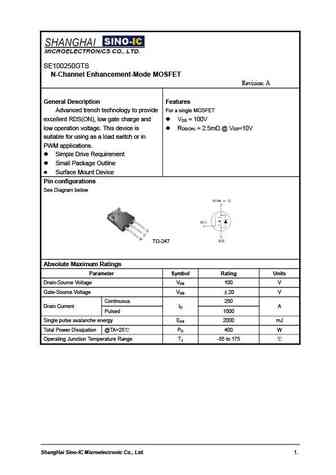
SE100250GTS N-Channel Enhancement-Mode MOSFET Revision A General Description Features For a single MOSFET Advanced trench technology to provide excellent RDS(ON), low gate charge and V = 100V DS low operation voltage. This device is R =2.5m @V =10V DS(ON) GS suitable for using as a load switch or in PWM applications. Simple Drive Requirement Small Package Outlin
9.10. Size:420K cn sino-ic
se10030a.pdf 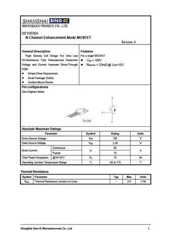
SE10030A N-Channel Enhancement-Mode MOSFET Revision A General Description Features Thigh Density Cell Design For Ultra Low For a single MOSFET On-Resistance Fully Characterized Avalanche V =100V DS Voltage and Current Improved Shoot-Through R =25m @V =10V DS(ON) GS FOM Simple Drive Requirement Small Package Outline Surface Mount Device Pin configurations
Другие IGBT... SE100130GA, SE10015, SE100150G, SE100180GA, SE100250GTS, SE1003, SE10030A, SE10060A, 4435, SE100P60, SE120120G, SE12060GA, SE1216, SE12N50FRA, SE12N65, SE138U, SE150110G