SE20040 Specs and Replacement
Type Designator: SE20040
Type of Transistor: MOSFET
Type of Control Channel: N-Channel
Absolute Maximum Ratings
Pd ⓘ - Maximum Power Dissipation: 220 W
|Vds|ⓘ - Maximum Drain-Source Voltage: 200 V
|Vgs|ⓘ - Maximum Gate-Source Voltage: 20 V
|Id| ⓘ - Maximum Drain Current: 40 A
Tj ⓘ - Maximum Junction Temperature: 175 °C
Electrical Characteristics
tr ⓘ - Rise Time: 24 nS
Cossⓘ - Output Capacitance: 290 pF
RDSonⓘ - Maximum Drain-Source On-State Resistance: 0.041 Ohm
Package: TO220
SE20040 substitution
- MOSFET ⓘ Cross-Reference Search
SE20040 datasheet
se20040.pdf
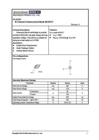
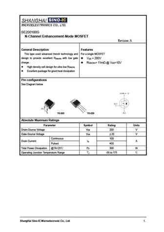
SE20040 N-Channel Enhancement-Mode MOSFET Revision A General Description Features For a single MOSFET Advanced trench technology to provide excellent RDS(ON), low gate charge and low V = 200V DS operation voltage. This device is suitable for R =36.4m @V =10V DS(ON) GS using as a load switch or in PWM applications. Simple Drive Requirement Small Package Outline ... See More ⇒
kse200.pdf
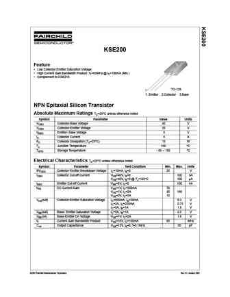
KSE200 Feature Low Collector-Emitter Saturation Voltage High Current Gain Bandwidth Product fT=65MHz @ IC=100mA (Min.) Complement to KSE210 TO-126 1 1. Emitter 2.Collector 3.Base NPN Epitaxial Silicon Transistor Absolute Maximum Ratings TC=25 C unless otherwise noted Symbol Parameter Value Units VCBO Collector-Base Voltage 40 V VCEO Collector-Emitter Voltage 25 V ... See More ⇒
kse200.pdf
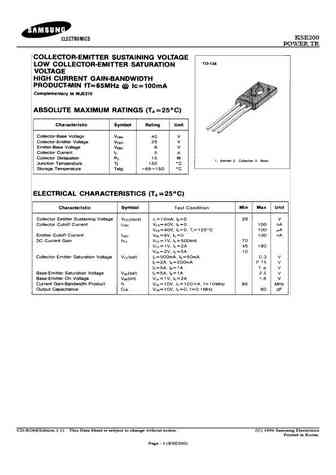
KSE200 POWER TR CD-ROM(Edition.1.1) This Data Sheet is subject to change without notice. (C) 1994 Samsung Electronics Printed in Korea. Page 1 (KSE200) KSE200 POWER TR CD-ROM(Edition.1.1) This Data Sheet is subject to change without notice. (C) 1994 Samsung Electronics Printed in Korea. Page 2 (KSE200) ... See More ⇒
Detailed specifications: SE150110G, SE150180G, SE150180GTS, SE15N50FRA, SE18NS65A, SE1991G, SE1991GA, SE200100G, AO3407, SE20075, SE2060, SE20N110, SE20P03, SE2101, SE2101E, SE2102M, SE2300
Keywords - SE20040 MOSFET specs
SE20040 cross reference
SE20040 equivalent finder
SE20040 pdf lookup
SE20040 substitution
SE20040 replacement
Step-by-step guide to finding a MOSFET replacement. Cross-reference parts and ensure compatibility for your repair or project.
🌐 : EN ES РУ

LIST
Last Update
MOSFET: AUB062N08BG | AUB060N08AG | AUB056N10 | AUB056N08BGL | AUB050N085 | AUB050N055 | AUB045N12 | AUB045N10BT | AUB039N10 | AUB034N10
Popular searches
2sc733 | a933 transistor | d209l | irfb4321 | 2n333 | c3852 | irfp140 | ksc2383 datasheet