25N06L-TN3 Specs and Replacement
Type Designator: 25N06L-TN3
Type of Transistor: MOSFET
Type of Control Channel: N-Channel
Absolute Maximum Ratings
Pd ⓘ - Maximum Power Dissipation: 100 W
|Vds|ⓘ - Maximum Drain-Source Voltage: 60 V
|Vgs|ⓘ - Maximum Gate-Source Voltage: 20 V
|Id| ⓘ - Maximum Drain Current: 35 A
Tj ⓘ - Maximum Junction Temperature: 175 °C
Electrical Characteristics
tr ⓘ - Rise Time: 15 nS
Cossⓘ - Output Capacitance: 140 pF
RDSonⓘ - Maximum Drain-Source On-State Resistance: 0.031 Ohm
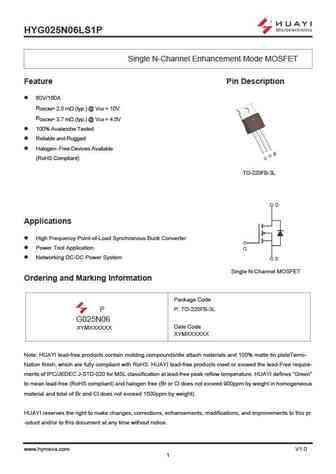
Package: TO252
25N06L-TN3 substitution
- MOSFET ⓘ Cross-Reference Search
25N06L-TN3 datasheet
25n06l-tn3.pdf
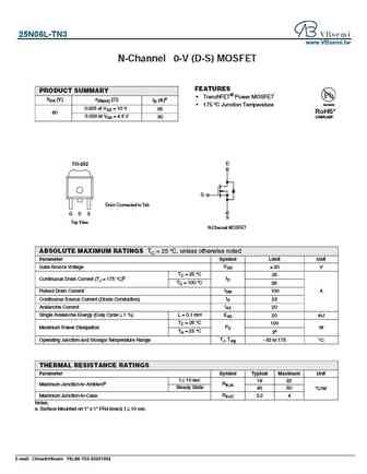
25N06L-TN3 www.VBsemi.tw N-Channel 6 0-V (D-S) MOSFET FEATURES PRODUCT SUMMARY TrenchFET Power MOSFET VDS (V) rDS(on) ( ) ID (A)a Available 175 C Junction Temperature 0.025 at VGS = 10 V 35 RoHS* 60 0.030 at VGS = 4.5 V 30 COMPLIANT TO-252 D G Drain Connected to Tab G D S S Top View N-Channel MOSFET ABSOLUTE MAXIMUM RATINGS TC = 25 C, unless otherwise no... See More ⇒
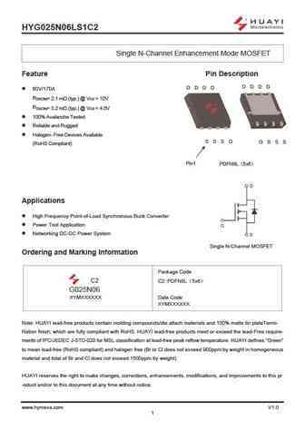
hyg025n06ls1c2.pdf
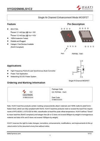
HYG025N06LS1C2 Single N-Channel Enhancement Mode MOSFET Feature Pin Description D D D D D D D D 60V/170A RDS(ON)= 2.1 m (typ.) @ VGS = 10V RDS(ON)= 3.2 m (typ.) @ VGS = 4.5V 100% Avalanche Tested Reliable and Rugged Halogen- Free Devices Available S S S G G S S S (RoHS Compliant) Pin1 PDFN8L 5x6 Applications High Frequency Point-of-Load Synchronous B... See More ⇒
php125n06lt 4.pdf
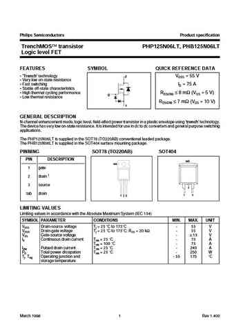
Philips Semiconductors Product specification TrenchMOS transistor PHP125N06LT, PHB125N06LT Logic level FET FEATURES SYMBOL QUICK REFERENCE DATA Trench technology VDSS = 55 V d Very low on-state resistance Fast switching ID = 75 A Stable off-state characteristics High thermal cycling performance RDS(ON) 8 m (VGS = 5 V) g Low thermal resistance... See More ⇒
phb125n06l.pdf
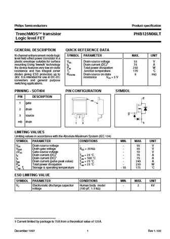
Philips Semiconductors Product specification TrenchMOS transistor PHB125N06LT Logic level FET GENERAL DESCRIPTION QUICK REFERENCE DATA N-channel enhancement mode logic SYMBOL PARAMETER MAX. UNIT level field-effect power transistor in a plastic envelope suitable for surface VDS Drain-source voltage 55 V mounting Using trench technology ID Drain current (DC)1 75 A the device fe... See More ⇒
Detailed specifications: 13N10, 15N10-TO251, 1812, 1N60L-TM3-T, 20N03L-TO252, 20N06L-TO252, 20N3LG-TO251, 20P06-TO252, K3569, 25NF20, 2N0623, 2N65-TO252, 2SJ530STL, 2SJ598-Z-E1, 2SK1589-T1B, 2SK1623, 2SK2158-T1B
Keywords - 25N06L-TN3 MOSFET specs
25N06L-TN3 cross reference
25N06L-TN3 equivalent finder
25N06L-TN3 pdf lookup
25N06L-TN3 substitution
25N06L-TN3 replacement
Need a MOSFET replacement? Our guide shows you how to find a perfect substitute by comparing key parameters and specs
History: STF16N60M6 | FHD70N03A | 2SK2148-01 | DMC4029SK4 | APM2300CA | SW1N60A | STB23N80K5
🌐 : EN ES РУ

LIST
Last Update
MOSFET: AUB034N10 | AUB033N08BG | AUB026N085 | AUA062N08BG | AUA060N08AG | AUA056N08BGL | AUA039N10 | ASW80R290E | ASW65R120EFD | ASW65R110E
Popular searches
2sa1283 | 2sb646 | 2sc1885 datasheet | 2sc2580 | 2sc710 | 2sc968 | 2sd217 | bdw93c equivalent