30P06 Specs and Replacement
Type Designator: 30P06
Type of Transistor: MOSFET
Type of Control Channel: P-Channel
Absolute Maximum Ratings
Pd ⓘ
- Maximum Power Dissipation: 113 W
|Vds|ⓘ - Maximum Drain-Source Voltage: 60 V
|Vgs|ⓘ - Maximum Gate-Source Voltage: 20 V
|Id| ⓘ - Maximum Drain Current: 50 A
Tj ⓘ - Maximum Junction Temperature: 150 °C
Electrical Characteristics
tr ⓘ - Rise Time: 70 nS
Cossⓘ -
Output Capacitance: 380 pF
RDSonⓘ - Maximum Drain-Source On-State Resistance: 0.025 Ohm
Package: TO252
- MOSFET ⓘ Cross-Reference Search
30P06 datasheet
..1. Size:820K cn vbsemi
30p06.pdf 
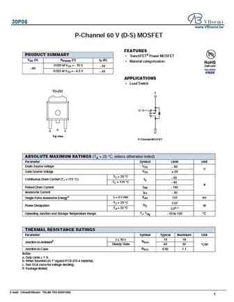
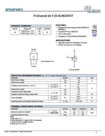
30P06 www.VBsemi.tw P-Channel 60 V (D-S) MOSFET FEATURES PRODUCT SUMMARY TrenchFET Power MOSFET VDS (V) RDS(on) ( )ID (A) Material categorization 0.020 at VGS = - 10 V - 50 - 60 0.025 at VGS = - 4.5 V - 45 APPLICATIONS Load Switch TO-252 S G D G S D Top View P-Channel MOSFET ABSOLUTE MAXIMUM RATINGS (TA = 25 C, unless otherwise noted) Parameter Symb... See More ⇒
0.1. Size:191K motorola
mtp30p06v .pdf

MOTOROLA Order this document SEMICONDUCTOR TECHNICAL DATA by MTP30P06V/D Designer's Data Sheet MTP30P06V TMOS V Motorola Preferred Device Power Field Effect Transistor P Channel Enhancement Mode Silicon Gate TMOS POWER FET TMOS V is a new technology designed to achieve an on resis- 30 AMPERES tance area product about one half that of standard MOSFETs. This 60 VOLTS new... See More ⇒
0.2. Size:215K motorola
mtb30p06v.pdf
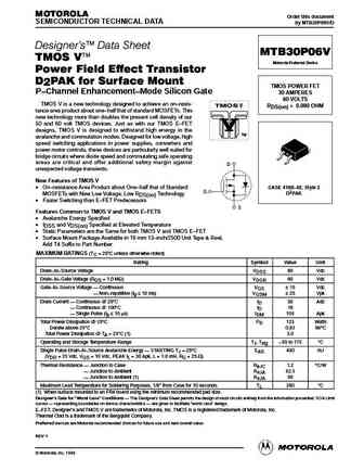
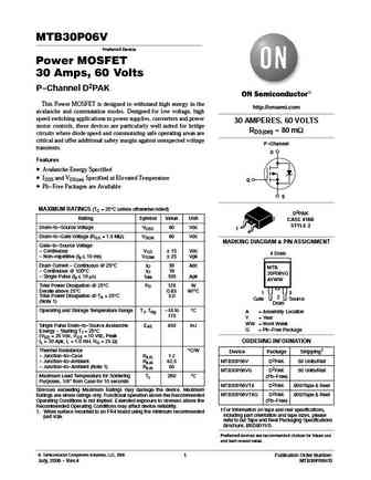
MOTOROLA Order this document SEMICONDUCTOR TECHNICAL DATA by MTB30P06V/D Designer's Data Sheet MTB30P06V TMOS V Motorola Preferred Device Power Field Effect Transistor D2PAK for Surface Mount TMOS POWER FET P Channel Enhancement Mode Silicon Gate 30 AMPERES 60 VOLTS TMOS V is a new technology designed to achieve an on resis- RDS(on) = 0.080 OHM tance area product abou... See More ⇒
0.3. Size:247K motorola
mtb30p06vrev1x.pdf

MOTOROLA Order this document SEMICONDUCTOR TECHNICAL DATA by MTB30P06V/D Designer's Data Sheet MTB30P06V TMOS V Motorola Preferred Device Power Field Effect Transistor D2PAK for Surface Mount TMOS POWER FET P Channel Enhancement Mode Silicon Gate 30 AMPERES 60 VOLTS TMOS V is a new technology designed to achieve an on resis- RDS(on) = 0.080 OHM tance area product abou... See More ⇒
0.4. Size:166K motorola
mtp30p06v.pdf
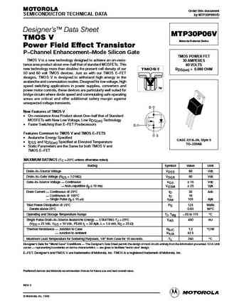
MOTOROLA Order this document SEMICONDUCTOR TECHNICAL DATA by MTP30P06V/D Designer's Data Sheet MTP30P06V TMOS V Motorola Preferred Device Power Field Effect Transistor P Channel Enhancement Mode Silicon Gate TMOS POWER FET TMOS V is a new technology designed to achieve an on resis- 30 AMPERES tance area product about one half that of standard MOSFETs. This 60 VOLTS new... See More ⇒
0.5. Size:386K fairchild semi
rfg30p06 rfp30p06 rf1s30p06sm.pdf
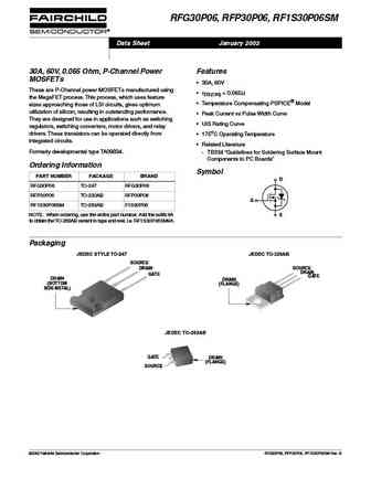
RFG30P06, RFP30P06, RF1S30P06SM Data Sheet January 2002 30A, 60V, 0.065 Ohm, P-Channel Power Features MOSFETs 30A, 60V These are P-Channel power MOSFETs manufactured using rDS(ON) = 0.065 the MegaFET process. This process, which uses feature Temperature Compensating PSPICE Model sizes approaching those of LSI circuits, gives optimum utilization of silicon, resultin... See More ⇒
0.6. Size:500K infineon
spd30p06p spd30p06pg.pdf
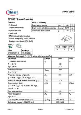
SPD30P06P G SIPMOS Power-Transistor Features Product Summary P-Channel Drain source voltage VDS -60 V Enhancement mode Drain-source on-state resistance RDS(on) 0.075 Avalanche rated Continuous drain current ID -30 A dv/dt rated 175 C operating temperature Pb-free lead plating; RoHS compliat Qualified according to AEC Q101 Pin 1 PIN 2/4 PIN 3 G D S Type Package S... See More ⇒
0.7. Size:81K onsemi
mtb30p06v mtb30p06vt4 mtb30p06vt4g.pdf
MTB30P06V Preferred Device Power MOSFET 30 Amps, 60 Volts P-Channel D2PAK This Power MOSFET is designed to withstand high energy in the http //onsemi.com avalanche and commutation modes. Designed for low voltage, high speed switching applications in power supplies, converters and power 30 AMPERES, 60 VOLTS motor controls, these devices are particularly well suited for bridge RDS(on) ... See More ⇒
0.8. Size:204K onsemi
mtp30p06v.pdf
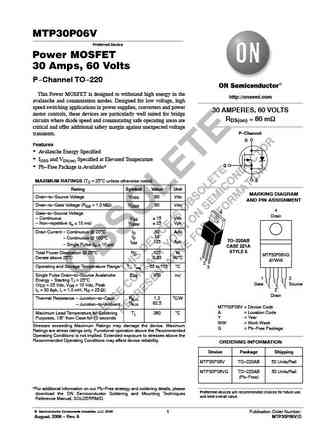
MTP30P06V Preferred Device Power MOSFET 30 Amps, 60 Volts P-Channel TO-220 This Power MOSFET is designed to withstand high energy in the http //onsemi.com avalanche and commutation modes. Designed for low voltage, high speed switching applications in power supplies, converters and power 30 AMPERES, 60 VOLTS motor controls, these devices are particularly well suited for bridge RDS(on)... See More ⇒
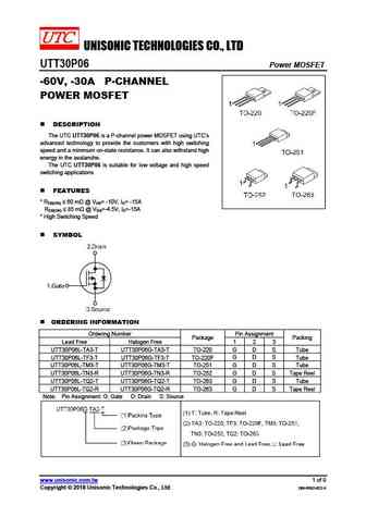
0.10. Size:132K utc
utt30p06.pdf
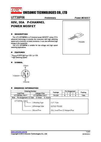
UNISONIC TECHNOLOGIES CO., LTD UTT30P06 Preliminary Power MOSFET 60V, 30A P-CHANNEL POWER MOSFET DESCRIPTION The UTC UTT30P06 is a P-channel power MOSFET using UTC s advanced technology to provide the customers with high switching speed and a minimum on-state resistance. It can also withstand high energy in the avalanche. The UTC UTT30P06 is suitable for low voltage and hi... See More ⇒
0.12. Size:44K harris semi
rf1s30p06.pdf
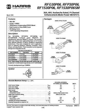
RFG30P06, RFP30P06, S E M I C O N D U C T O R RF1S30P06, RF1S30P06SM 30A, 60V, Avalanche Rated, P-Channel March 1995 Enhancement-Mode Power MOSFETs Features Packages JEDEC STYLE TO-247 30A, 60V SOURCE rDS(ON) = 0.065 DRAIN GATE Temperature Compensating PSPICE Model DRAIN Peak Current vs Pulse WIdth Curve (BOTTOM SIDE METAL) UIS Rating Curve +175oC Op... See More ⇒
0.13. Size:304K analog power
am30p06-40d.pdf
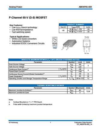
Analog Power AM30P06-40D P-Channel 60-V (D-S) MOSFET PRODUCT SUMMARY Key Features rDS(on) (m ) VDS (V) ID (A) Low r trench technology DS(on) 40 @ VGS = -10V -29 Low thermal impedance -60 55 @ VGS = -4.5V -25 Fast switching speed Typical Applications White LED boost converters Automotive Systems Industrial DC/DC Conversion Circuits ABSOLUTE MAX... See More ⇒
0.14. Size:138K analog power
am30p06-45d.pdf
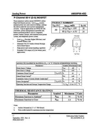
Analog Power AM30P06-45D P-Channel 60-V (D-S) MOSFET These miniature surface mount MOSFETs utilize High Cell Density process. Low rDS(on) assures PRODUCT SUMMARY minimal power loss and conserves energy, making VDS (V) rDS(on) m( )ID (A) this device ideal for use in power management 49 @ VGS = -10V 28 circuitry. Typical applications are PWM DC-DC -60 converters, power management ... See More ⇒
0.15. Size:280K cystek
mtb30p06j3.pdf
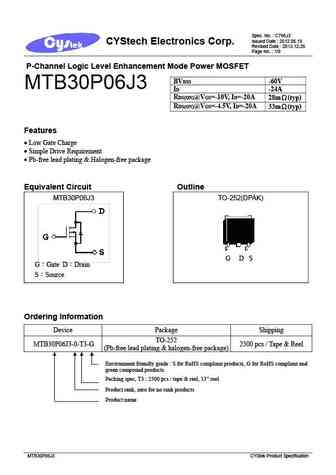
Spec. No. C796J3 Issued Date 2012.06.19 CYStech Electronics Corp. Revised Date 2013.12.26 Page No. 1/9 P-Channel Logic Level Enhancement Mode Power MOSFET BVDSS -60V MTB30P06J3 ID -24A RDS(ON)@VGS=-10V, ID=-20A 28m (typ) RDS(ON)@VGS=-4.5V, ID=-20A 33m (typ) Features Low Gate Charge Simple Drive Requirement Pb-free lead plating & Halogen-free packag... See More ⇒
0.16. Size:1102K blue-rocket-elect
brd30p06.pdf
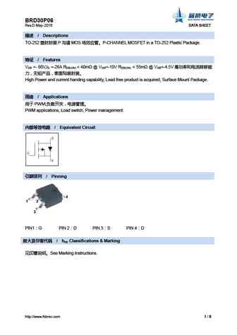
BRD30P06 Rev.D May.-2016 DATA SHEET / Descriptions TO-252 P MOS P-CHANNEL MOSFET in a TO-252 Plastic Package. / Features VDS =- 60V,ID =-26A RDS(ON) ... See More ⇒
0.17. Size:550K bruckewell
msd30p06.pdf
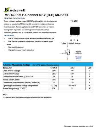
MSD30P06 P-Channel 60-V (D-S) MOSFET GENERAL DESCRIPTION These miniature surface mount MOSFETs utilize a high cell density trench process to provide low RDS(on) and to ensure minimal power loss and heat dissipation. Typical applications are DC-DC converters and power management in portable and battery-powered products such as computers, printers, and PCMCIA cards, cellular and cord... See More ⇒
0.18. Size:264K ncepower
nce30p06j.pdf
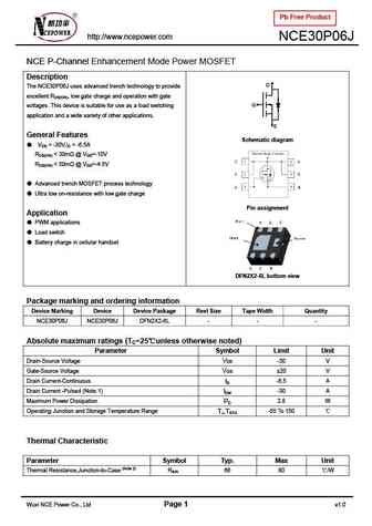
Pb Free Product http //www.ncepower.com NCE30P06J NCE P-Channel Enhancement Mode Power MOSFET Description D The NCE30P06J uses advanced trench technology to provide excellent RDS(ON), low gate charge and operation with gate G voltages .This device is suitable for use as a load switching application and a wide variety of other applications. S General Features Schematic diag... See More ⇒
0.21. Size:1134K winsok
wsf30p06.pdf
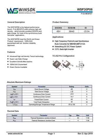
WSF30P06 P-Ch MOSFET General Description Product Summery The WSF30P06 is the highest performance BVDSS RDSON ID trench P-ch MOSFETs with extreme high cell density , which provide excellent RDSON and -60V 38m -23.5A gate charge for most of the synchronous buck converter applications . Applications The WSF30P06 meet the RoHS and Green Product requirement , 100% EAS High F... See More ⇒
0.22. Size:840K cn vbsemi
rfp30p06.pdf
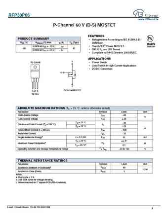
RFP30P06 www.VBsemi.tw P-Channel 60 V (D-S) MOSFET FEATURES PRODUCT SUMMARY Halogen-free According to IEC 61249-2-21 VDS (V) RDS(on) ( ) Max. ID (A) Qg (Typ.) Definition TrenchFET Power MOSFET 0.0600 at VGS = - 10 V - 30 - 60 67 100 % Rg and UIS Tested 0.0850 at VGS = - 4.5 V - 24 Compliant to RoHS Directive 2002/95/EC APPLICATIONS S TO-220AB Power Swi... See More ⇒
0.23. Size:845K cn vbsemi
spd30p06pg.pdf
SPD30P06PG www.VBsemi.tw P-Channel 60 V (D-S) MOSFET FEATURES PRODUCT SUMMARY Halogen-free According to IEC 61249-2-21 VDS (V) RDS(on) ( ) ID (A)d Qg (Typ) Definition 0.053 at VGS = - 10 V - 25 TrenchFET Power MOSFET - 60 26 0.062 at VGS = - 4.5 V - 20 100 % UIS Tested Compliant to RoHS Directive 2002/95/EC APPLICATIONS High Side Switch for Full Bridge C... See More ⇒
0.24. Size:1655K cn apm
ap30p06d.pdf
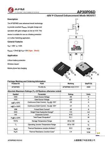
AP30P06D -60V P-Channel Enhancement Mode MOSFET Description The AP30P06D uses advanced trench technology to provide excellent R , low gate charge and DS(ON) operation with gate voltages as low as 4.5V. This device is suitable for use as a Battery protection or in other Switching application. General Features V = -60V I =-30A DS D R ... See More ⇒
Detailed specifications: 2SJ598-Z-E1, 2SK1589-T1B, 2SK1623, 2SK2158-T1B, 30N06L, 30N06-TO220, 30N06-TO252, 30N20, IRF530, 70N06L-TQ2, 80N10, AF2301PWL, AF4502CSLA, AFN3404S23RG, AFN4172WSS8, AFP2307AS23, AM20P06-135
Keywords - 30P06 MOSFET specs
30P06 cross reference
30P06 equivalent finder
30P06 pdf lookup
30P06 substitution
30P06 replacement
Can't find your MOSFET?
Learn how to find a substitute transistor by analyzing voltage, current and package compatibility