APM7313KC Specs and Replacement
Type Designator: APM7313KC
Type of Transistor: MOSFET
Type of Control Channel: N-Channel
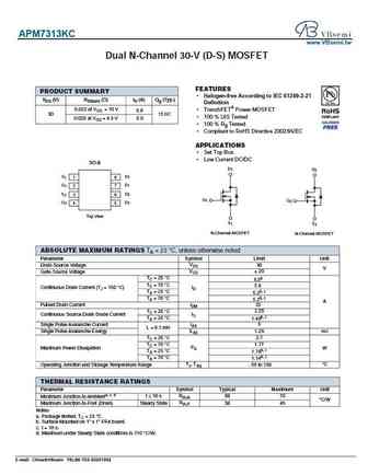
Absolute Maximum Ratings
Pd ⓘ - Maximum Power Dissipation: 1.78 W
|Vds|ⓘ - Maximum Drain-Source Voltage: 30 V
|Vgs|ⓘ - Maximum Gate-Source Voltage: 20 V
|Id| ⓘ - Maximum Drain Current: 6.2 A
Tj ⓘ - Maximum Junction Temperature: 150 °C
Electrical Characteristics
tr ⓘ - Rise Time: 55 nS
Cossⓘ - Output Capacitance: 117 pF
RDSonⓘ - Maximum Drain-Source On-State Resistance: 0.022 typ Ohm
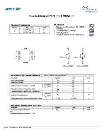
Package: SO8
APM7313KC substitution
- MOSFET ⓘ Cross-Reference Search
APM7313KC datasheet
apm7313k.pdf
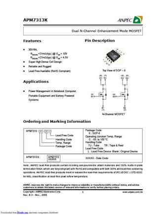
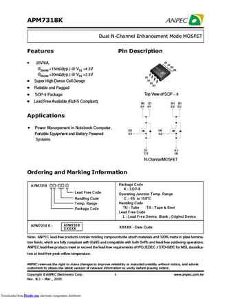
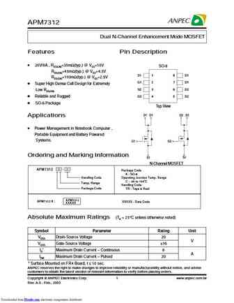
APM7313K Dual N-Channel Enhancement Mode MOSFET Pin Description Features 30V/6A, RDS(ON) =21m (typ.) @ VGS = 10V RDS(ON) =27m (typ.) @ VGS = 4.5V Super High Dense Cell Design Reliable and Rugged Top View of SOP - 8 Lead Free Available (RoHS Compliant) (8) (7) (6) (5) D1 D1 D2 D2 Applications Power Management in Notebook Computer, (2) (4) Portable Equipment and Battery P... See More ⇒
apm7318.pdf
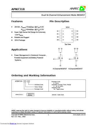
APM7318 Dual N-Channel Enhancement Mode MOSFET Features Pin Description 20V/8A , RDS(ON)=15m (typ.) @ VGS=4.5V SO-8 RDS(ON)=30m (typ.) @ VGS=2.5V S1 1 8 D1 Super High Dense Cell Design for Extremely G1 2 7 D1 Low RDS(ON) S2 3 6 D2 Reliable and Rugged G2 45 D2 SO-8 Package Top View D1 D1 D2 D2 Applica... See More ⇒

Detailed specifications: APM4050PUC, APM4303KC, APM4330KC, APM4532KC, APM4550KC, APM4828KC-TRL, APM4927KC, APM4953KC, P55NF06, APM7318KC, APM8010KC, APM9435KC, APM9945KC, BSC019N04NS, BUK9832-55, C3028LD, CEA3055
Keywords - APM7313KC MOSFET specs
APM7313KC cross reference
APM7313KC equivalent finder
APM7313KC pdf lookup
APM7313KC substitution
APM7313KC replacement
Step-by-step guide to finding a MOSFET replacement. Cross-reference parts and ensure compatibility for your repair or project.
🌐 : EN ES РУ

LIST
Last Update
MOSFET: AUB034N10 | AUB033N08BG | AUB026N085 | AUA062N08BG | AUA060N08AG | AUA056N08BGL | AUA039N10 | ASW80R290E | ASW65R120EFD | ASW65R110E
Popular searches
c1841 transistor | fb42n20d | irfb3306 equivalent | irfp460 характеристики | k2837 datasheet | k389 transistor | mje15032g equivalent | nsd134