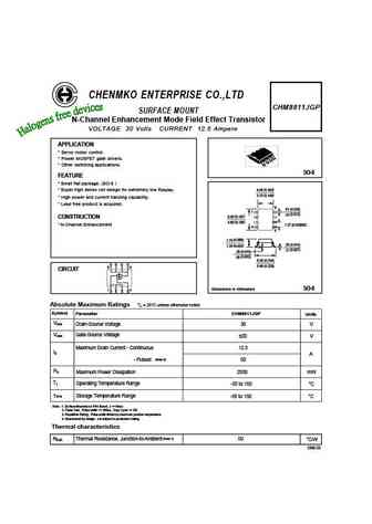
HM8810E Specs and Replacement
Type Designator: HM8810E
Type of Transistor: MOSFET
Type of Control Channel: N-Channel
Absolute Maximum Ratings
Pd ⓘ - Maximum Power Dissipation: 1 W
|Vds|ⓘ - Maximum Drain-Source Voltage: 20 V
|Vgs|ⓘ - Maximum Gate-Source Voltage: 12 V
|Id| ⓘ - Maximum Drain Current: 5.2 A
Tj ⓘ - Maximum Junction Temperature: 150 °C
Electrical Characteristics
tr ⓘ - Rise Time: 330 nS
RDSonⓘ - Maximum Drain-Source On-State Resistance: 0.024 typ Ohm
Package: TSOP6
HM8810E substitution
- MOSFET ⓘ Cross-Reference Search
HM8810E datasheet
hm8810e.pdf
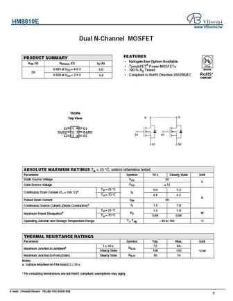
HM8810E www.VBsemi.tw Dual N-Channel MOSFET FEATURES PRODUCT SUMMARY Halogen-free Option Available VDS (V) RDS(on) ( )ID (A) Pb-free TrenchFET Power MOSFETs 0.024 at VGS = 4.5 V Available 6.0 100 % Rg Tested 20 RoHS* 0.028 at VGS = 2.5 V Compliant to RoHS Directive 2002/95/EC 5.0 COMPLIANT TSOP6 D D Top View S1 1 6 G1 D1/D2 2 5 D1/D2 G1 G2 S2 G2 3 4... See More ⇒
hm8810e.pdf
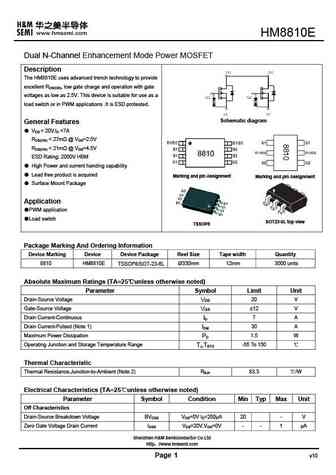
HM8810E Dual N-Channel Enhancement Mode Power MOSFET Description The HM8810E uses advanced trench technology to provide excellent RDS(ON), low gate charge and operation with gate voltages as low as 2.5V. This device is suitable for use as a load switch or in PWM applications .It is ESD protested. Schematic diagram General Features VDS = 20V,ID =7A RDS(ON) ... See More ⇒
hm8810s.pdf
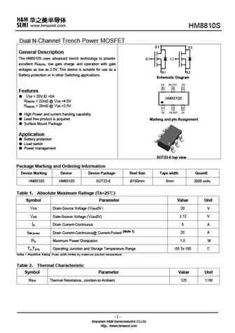
HM8810S Dual N-Channel Trench Power MOSFET General Description The HM8810S uses advanced trench technology to provide excellent R , low gate charge and operation with gate DS(ON) voltages as low as 2.5V. This device is suitable for use as a Battery protection or in other Switching applications. Schematic Diagram Features VDS = 20V,ID =5A HM8810S R ... See More ⇒
hm8810a.pdf
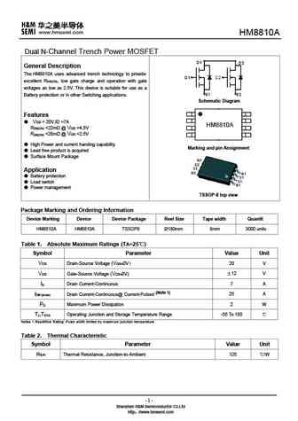
HM Dual N-Channel Trench Power MOSFET General Description The HM uses advanced trench technology to provide excellent R , low gate charge and operation with gate DS(ON) voltages as low as 2.5V. This device is suitable for use as a Battery protection or in other Switching applications. Schematic Diagram Features VDS = 20V,ID =7A HM R ... See More ⇒
Detailed specifications: HM2305PR, HM2310, HM2310PR, HM25P06K, HM3400PR, HM4409, HM4410, HM70P04K, SPP20N60C3, HS50N06DA, IM2132, IM4435G, IPP048N04, IPP048N06, IRF3410, IRF4435TR, IRF5305STR
Keywords - HM8810E MOSFET specs
HM8810E cross reference
HM8810E equivalent finder
HM8810E pdf lookup
HM8810E substitution
HM8810E replacement
Learn how to find the right MOSFET substitute. A guide to cross-reference, check specs and replace MOSFETs in your circuits.
🌐 : EN ES РУ

LIST
Last Update
MOSFET: AUN084N10 | AUN065N10 | AUN063N10 | AUN062N08BG | AUN060N08AG | AUN053N10 | AUN050N08BGL | AUN045N085 | AUN042N055 | AUN036N10
Popular searches
2n3773 | b772 transistor | 50n06 | mje350 | 2n3866 | irf 3205 | 2n5088 equivalent | d882 transistor