ME20N10 Specs and Replacement
Type Designator: ME20N10
Type of Transistor: MOSFET
Type of Control Channel: N-Channel
Absolute Maximum Ratings
Pd ⓘ - Maximum Power Dissipation: 96 W
|Vds|ⓘ - Maximum Drain-Source Voltage: 100 V
|Vgs|ⓘ - Maximum Gate-Source Voltage: 20 V
|Id| ⓘ - Maximum Drain Current: 15 A
Tj ⓘ - Maximum Junction Temperature: 175 °C
Electrical Characteristics
tr ⓘ - Rise Time: 50 nS
Cossⓘ - Output Capacitance: 120 pF
RDSonⓘ - Maximum Drain-Source On-State Resistance: 0.114 typ Ohm
Package: TO252
ME20N10 substitution
- MOSFET ⓘ Cross-Reference Search
ME20N10 datasheet
me20n10 me20n10-g.pdf
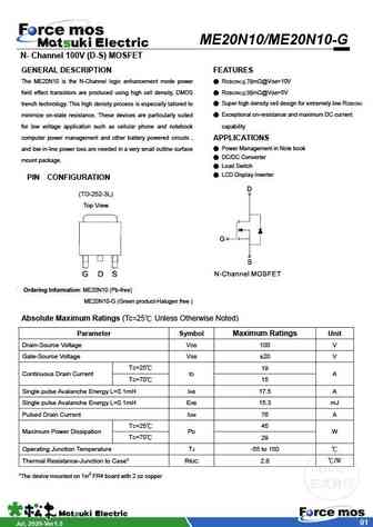
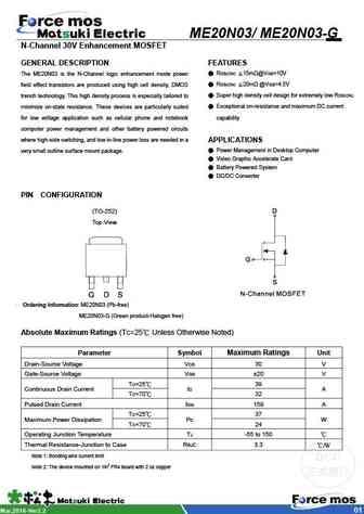
ME20N10/ME20N10-G N- Channel 100V (D-S) MOSFET GENERAL DESCRIPTION FEATURES The ME20N10 is the N-Channel logic enhancement mode power RDS(ON) 78m @VGS=10V field effect transistors are produced using high cell density, DMOS RDS(ON) 98m @VGS=5V trench technology. This high density process is especially tailored to Super high density cell design for extremely low RDS(ON)... See More ⇒
me20n10.pdf
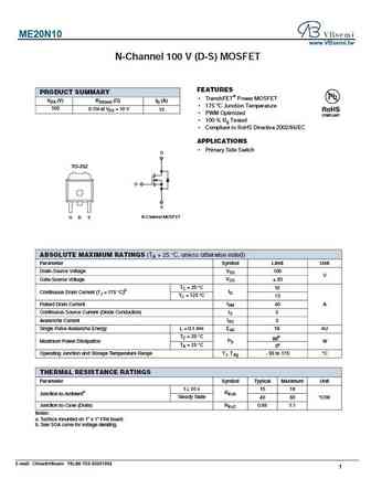
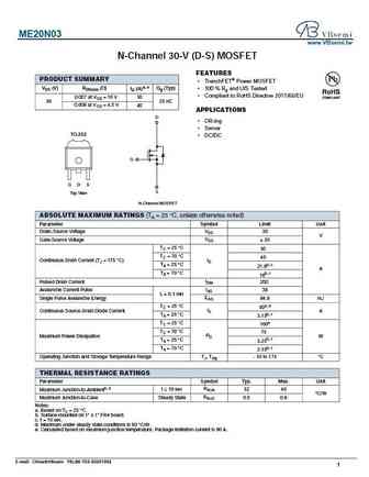
ME20N10 www.VBsemi.tw N-Channel 100 V (D-S) MOSFET FEATURES PRODUCT SUMMARY TrenchFET Power MOSFET VDS (V) RDS(on) ( )ID (A) 175 C Junction Temperature 100 0.11 4 at VGS = 10 V 15 PWM Optimized 100 % Rg Tested Compliant to RoHS Directive 2002/95/EC APPLICATIONS Primary Side Switch D TO-252 G S G D S N-Channel MOSFET ABSOLUTE MAXIMUM RATINGS (... See More ⇒
me20n15 me20n15-g.pdf
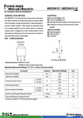
ME20N15 / ME20N15-G N- Channel 150V (D-S) MOSFET GENERAL DESCRIPTION FEATURES RDS(ON) 90m @VGS=10V The ME20N15 is the N-Channel logic enhancement mode power RDS(ON) 110m @VGS=7V field effect transistors are produced using high cell density, DMOS Super high density cell design for extremely low RDS(ON) trench technology. This high density process is especially t... See More ⇒
me20n15f.pdf
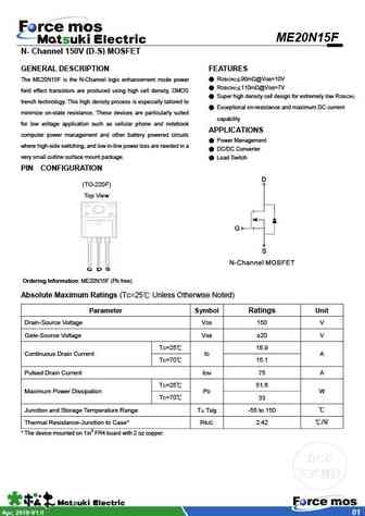
ME20N15F N- Channel 150V (D-S) MOSFET GENERAL DESCRIPTION FEATURES RDS(ON) 90m @VGS=10V The ME20N15F is the N-Channel logic enhancement mode power RDS(ON) 110m @VGS=7V field effect transistors are produced using high cell density, DMOS Super high density cell design for extremely low RDS(ON) trench technology. This high density process is especially tailored to... See More ⇒
Detailed specifications: KD3422A, KD4953, LR024N, LR8103V, LU120N, MDD1653RH, MDU2657RH, MDV1595SU, K4145, ME4410, MEM2301, MEM2302, MI4800, MMBF0201NLT1G, MMDF3P03HDR, MT2300ACTR, MT4435ACTR
Keywords - ME20N10 MOSFET specs
ME20N10 cross reference
ME20N10 equivalent finder
ME20N10 pdf lookup
ME20N10 substitution
ME20N10 replacement
Can't find your MOSFET? Learn how to find a substitute transistor by analyzing voltage, current and package compatibility
History: 2SK749 | SIHFD123 | OSG65R1K4AF | APM2305AC | TK50A04K3 | SRC60R125B | SRC60R075FBS
🌐 : EN ES РУ

LIST
Last Update
MOSFET: AUB062N08BG | AUB060N08AG | AUB056N10 | AUB056N08BGL | AUB050N085 | AUB050N055 | AUB045N12 | AUB045N10BT | AUB039N10 | AUB034N10
Popular searches
2n3904 transistor equivalent | 2sc2312 | bu406 datasheet | irfb7437 | tip32a | p75nf75 mosfet equivalent | irfpe50 | tip50