MTD20N03HDLT4G Specs and Replacement
Type Designator: MTD20N03HDLT4G
Type of Transistor: MOSFET
Type of Control Channel: N-Channel
Absolute Maximum Ratings
Pd ⓘ - Maximum Power Dissipation: 100 W
|Vds|ⓘ - Maximum Drain-Source Voltage: 30 V
|Vgs|ⓘ - Maximum Gate-Source Voltage: 20 V
|Id| ⓘ - Maximum Drain Current: 50 A
Tj ⓘ - Maximum Junction Temperature: 175 °C
Electrical Characteristics
tr ⓘ - Rise Time: 11 nS
Cossⓘ - Output Capacitance: 525 pF
RDSonⓘ - Maximum Drain-Source On-State Resistance: 0.007 typ Ohm
Package: TO252
MTD20N03HDLT4G substitution
- MOSFET ⓘ Cross-Reference Search
MTD20N03HDLT4G datasheet
mtd20n03hdlt4g.pdf
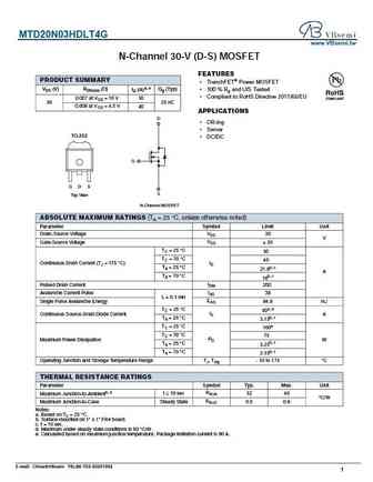
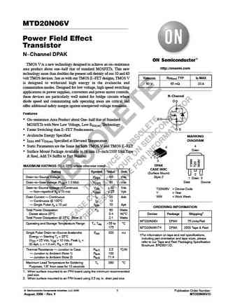
MTD20N03HDLT4G www.VBsemi.tw N-Channel 30-V (D-S) MOSFET FEATURES PRODUCT SUMMARY TrenchFET Power MOSFET VDS (V) RDS(on) ( ) ID (A)a, e Qg (Typ) 100 % Rg and UIS Tested Compliant to RoHS Directive 2011/65/EU 0.007 at VGS = 10 V 50 30 25 nC 0.009 at VGS = 4.5 V 40 APPLICATIONS D OR-ing Server TO-252 DC/DC G G D S S Top View N-Channel MOSFET ... See More ⇒
mtd20n03hdl.pdf

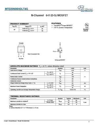
MOTOROLA Order this document SEMICONDUCTOR TECHNICAL DATA by MTD20N03HDL/D Designer's Data Sheet MTD20N03HDL HDTMOS E-FET. Motorola Preferred Device High Density Power FET TMOS POWER FET DPAK for Surface Mount LOGIC LEVEL N Channel Enhancement Mode Silicon Gate 20 AMPERES 30 VOLTS This advanced HDTMOS power FET is designed to withstand RDS(on) = 0.035 OHM high energy... See More ⇒
mtd20n03hd.pdf
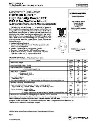
MOTOROLA Order this document SEMICONDUCTOR TECHNICAL DATA by MTD20N03HDL/D Designer's Data Sheet MTD20N03HDL HDTMOS E-FET. Motorola Preferred Device High Density Power FET TMOS POWER FET DPAK for Surface Mount LOGIC LEVEL N Channel Enhancement Mode Silicon Gate 20 AMPERES 30 VOLTS This advanced HDTMOS power FET is designed to withstand RDS(on) = 0.035 OHM high energy... See More ⇒
mtd20n06v.pdf
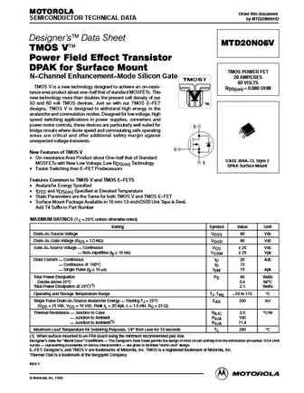
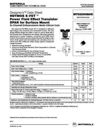
MOTOROLA Order this document SEMICONDUCTOR TECHNICAL DATA by MTD20N06V/D Designer's Data Sheet MTD20N06V TMOS V Power Field Effect Transistor DPAK for Surface Mount TMOS POWER FET N Channel Enhancement Mode Silicon Gate 20 AMPERES 60 VOLTS TMOS V is a new technology designed to achieve an on resis- RDS(on) = 0.080 OHM tance area product about one half that of standa... See More ⇒


Detailed specifications: MEM2302, MI4800, MMBF0201NLT1G, MMDF3P03HDR, MT2300ACTR, MT4435ACTR, MT4606, MT6680, AON7506, MTD20N06HDLT4G, MTD3055EL, MTP60N06HD, MTP8N06, N3PF06, NCE0117, NCE3010S, NCE3035G
Keywords - MTD20N03HDLT4G MOSFET specs
MTD20N03HDLT4G cross reference
MTD20N03HDLT4G equivalent finder
MTD20N03HDLT4G pdf lookup
MTD20N03HDLT4G substitution
MTD20N03HDLT4G replacement
Need a MOSFET replacement? Our guide shows you how to find a perfect substitute by comparing key parameters and specs
🌐 : EN ES РУ

LIST
Last Update
MOSFET: AUB034N10 | AUB033N08BG | AUB026N085 | AUA062N08BG | AUA060N08AG | AUA056N08BGL | AUA039N10 | ASW80R290E | ASW65R120EFD | ASW65R110E
Popular searches
irfbc40 | mp16b transistor | 2sa934 | 2sd118 | 2n3403 | 2sa750 | tip117 | 2n3643