VBFB1101M Datasheet. Specs and Replacement
Type Designator: VBFB1101M 📄📄
Type of Transistor: MOSFET
Type of Control Channel: N-Channel
Absolute Maximum Ratings
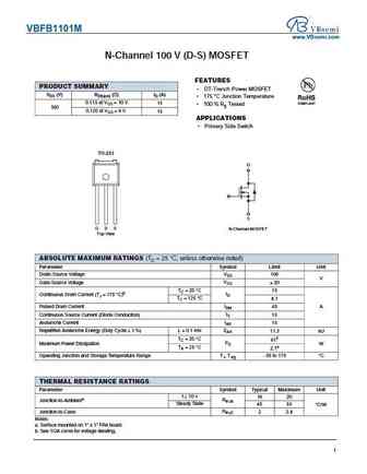
Pd ⓘ - Maximum Power Dissipation: 61 W
|Vds|ⓘ - Maximum Drain-Source Voltage: 100 V
|Vgs|ⓘ - Maximum Gate-Source Voltage: 20 V
|Id| ⓘ - Maximum Drain Current: 15 A
Tj ⓘ - Maximum Junction Temperature: 175 °C
Electrical Characteristics
tr ⓘ - Rise Time: 35 nS
Cossⓘ - Output Capacitance: 110 pF
RDSonⓘ - Maximum Drain-Source On-State Resistance: 0.110 typ Ohm
Package: TO251
📄📄 Copy
- MOSFET ⓘ Cross-Reference Search
VBFB1101M datasheet
..1. Size:784K cn vbsemi
vbfb1101m.pdf 

VBFB1101M www.VBsemi.com N-Channel 100 V (D-S) MOSFET FEATURES PRODUCT SUMMARY DT-Trench Power MOSFET VDS (V) RDS(on) ( )ID (A) 175 C Junction Temperature 0.115 at VGS = 10 V 15 100 % Rg Tested 100 0.120 at VGS = 6 V 15 APPLICATIONS Primary Side Switch TO-251 D G S G D S N-Channel MOSFET Top View ABSOLUTE MAXIMUM RATINGS (TC = 25 C, unless otherwi... See More ⇒
7.1. Size:567K cn vbsemi
vbfb1102m.pdf 

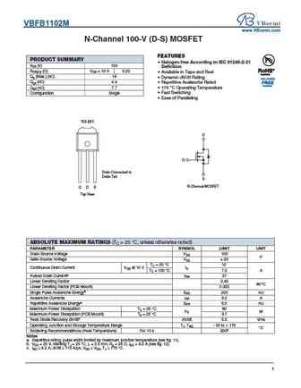
VBFB1102M www.VBsemi.com N-Channel 100-V (D-S) MOSFET FEATURES PRODUCT SUMMARY Halogen-free According to IEC 61249-2-21 VDS (V) 100 Definition RDS(on) ( )VGS = 10 V 0.20 Available in Tape and Reel Available Qg (Max.) (nC) 16 Dynamic dV/dt Rating Qgs (nC) 4.4 Repetitive Avalanche Rated Available Qgd (nC) 7.7 175 C Operating Temperature Configuration Sin... See More ⇒
7.2. Size:717K cn vbsemi
vbfb1104n.pdf 

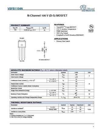
VBFB1104N www.VBsemi.com N-Channel 100 V (D-S) MOSFET FEATURES PRODUCT SUMMARY TrenchFET Power MOSFET VDS (V) RDS(on) ( )ID (A) 175 C Junction Temperature 100 0.036 at VGS = 10 V 35 PWM Optimized 100 % Rg Tested Compliant to RoHS Directive 2002/95/EC TO-251 APPLICATIONS Primary Side Switch D G S G D S N-Channel MOSFET Top View ABSOLUTE MAXI... See More ⇒
9.1. Size:778K cn vbsemi
vbfb1303.pdf 

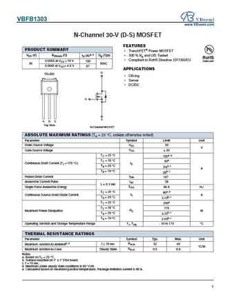
VBFB1303 www.VBsemi.com N-Channel 30-V (D-S) MOSFET FEATURES PRODUCT SUMMARY TrenchFET Power MOSFET VDS (V) RDS(on) ( ) ID (A)a, e Qg (Typ) 100 % Rg and UIS Tested Compliant to RoHS Directive 2011/65/EU 0.0035 at VGS = 10 V 100 30 95nC 0.0045 at VGS = 4.5 V 97 APPLICATIONS D TO-251 OR-ing Server DC/DC G S G D S Top View N-Channel MOSFET AB... See More ⇒
9.2. Size:932K cn vbsemi
vbm165r07 vbmb165r07 vbe165r07 vbfb165r07.pdf 

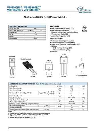
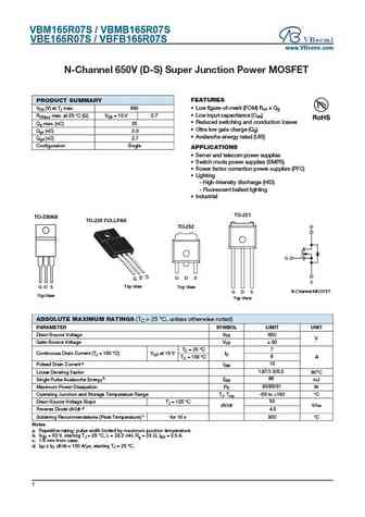
VBM165R07 / VBMB165R07 VBE165R07 / VBFB165R07 www.VBsemi.com N hannel 650 D S Power MOSFET FEATURES PRODUCT SUMMARY VDS (V) at TJ max. 650 Low figure-of-merit (FOM) Ron x Qg Low input capacitance (Ciss) RDS(on) max. at 25 C ( ) VGS = 10 V 1.1 Reduced switching and conduction losses Qg max. (nC) 25 Ultra low gate charge (Qg) Qgs (nC) 2.0 Avalanche energy r... See More ⇒
9.3. Size:802K cn vbsemi
vbfb1410.pdf 

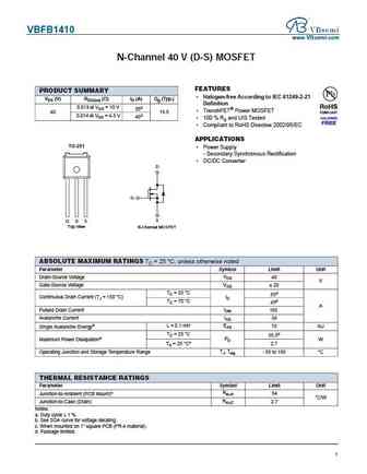
VBFB1410 www.VBsemi.com N-Channel 40 V (D-S) MOSFET FEATURES PRODUCT SUMMARY Halogen-free According to IEC 61249-2-21 VDS (V) RDS(on) ( ) ID (A) Qg (Typ.) Definition 0.0 3 at VGS = 10 V 55d TrenchFET Power MOSFET 40 9.5 0.0 at VGS = 4.5 V 5d 100 % Rg and UIS Tested Compliant to RoHS Directive 2002/95/EC APPLICATIONS TO-251 Power Supply - Secondary ... See More ⇒
9.4. Size:586K cn vbsemi
vbfb1630.pdf 

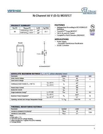
VBFB1630 www.VBsemi.com N-Channel 60 V (D-S) MOSFET FEATURES PRODUCT SUMMARY Halogen-free According to IEC 61249-2-21 VDS (V) RDS(on) ( ) ID (A) Qg (Typ.) Definition 0.032 at VGS = 10 V 35d TrenchFET Power MOSFET 60 21.7 0.037 at VGS = 4.5 V 30d 100 % Rg and UIS Tested Compliant to RoHS Directive 2002/95/EC APPLICATIONS Power Supply D TO-251 - Seconda... See More ⇒
9.5. Size:733K cn vbsemi
vbfb1405.pdf 

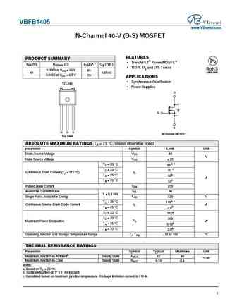
VBFB1405 www.VBsemi.com N-Channel 40-V (D-S) MOSFET FEATURES PRODUCT SUMMARY TrenchFET Power MOSFET VDS (V) RDS(on) ( ) ID (A)a, c Qg (Typ.) 100 % Rg and UIS Tested RoHS 0.0050 at VGS = 10 V 85 COMPLIANT 40 120 nC 0.0065 at VGS = 4.5 V 70 APPLICATIONS Synchronous Rectification TO-251 Power Supplies D G S G D S N-Channel MOSFET Top View ABSOLUTE M... See More ⇒
9.6. Size:722K cn vbsemi
vbfb1203m.pdf 

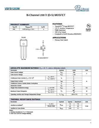
VBFB1203M www.VBsemi.com N-Channel 200 V (D-S) MOSFET FEATURES PRODUCT SUMMARY TrenchFET Power MOSFET VDS (V) RDS(on) ( )ID (A) 175 C Junction Temperature 200 0.270 at VGS = 10 V 8 PWM Optimized 100 % Rg Tested Compliant to RoHS Directive 2002/95/EC TO-251 APPLICATIONS Primary Side Switch D G S G D S N-Channel MOSFET Top View ABSOLUTE MAXIMU... See More ⇒
9.7. Size:1284K cn vbsemi
vbm165r10 vbmb165r10 vbe165r10 vbfb165r10.pdf 

VBM165R10 / VBMB165R10 VBE165R10 / VBFB165R10 www.VBsemi.com N hannel 650 D S Power MOSFET FEATURES PRODUCT SUMMARY VDS (V) at TJ max. 650 Low figure-of-merit (FOM) Ron x Qg Low input capacitance (Ciss) RDS(on) max. at 25 C ( ) VGS = 10 V 0.9 Reduced switching and conduction losses Qg max. (nC) 57 Ultra low gate charge (Qg) Qgs (nC) 4.0 Avalanche energy... See More ⇒
9.8. Size:543K cn vbsemi
vbfb1208n.pdf 

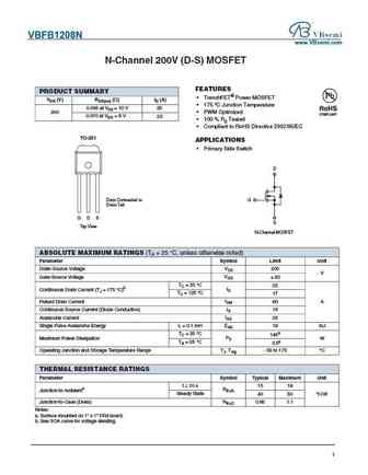
VBFB1208N www.VBsemi.com N-Channel 200V (D-S) MOSFET FEATURES PRODUCT SUMMARY TrenchFET Power MOSFET VDS (V) RDS(on) ( )ID (A) 175 C Junction Temperature 0.056 at VGS = 10 V 25 PWM Optimized 200 0.070 at VGS = 6 V 23 100 % Rg Tested Compliant to RoHS Directive 2002/95/EC TO-251 APPLICATIONS Primary Side Switch D Drain Connected to G Dr... See More ⇒
9.10. Size:1223K cn vbsemi
vbfb165r04.pdf 

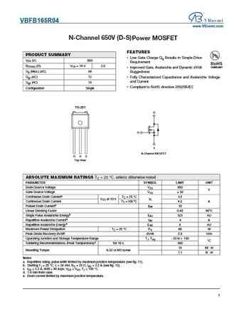
VBFB165R04 www.VBsemi.com N hannel 650 D S Power MOSFET FEATURES PRODUCT SUMMARY Low Gate Charge Qg Results in Simple Drive VDS (V) 650 Requirement RoHS RDS(on) ( )VGS = 10 V 2.0 COMPLIANT Improved Gate, Avalanche and Dynamic dV/dt Qg (Max.) (nC) 48 Ruggedness Qgs (nC) 12 Fully Characterized Capacitance and Avalanche Voltage and Current Qgd (nC) 19 Comp... See More ⇒
9.11. Size:765K cn vbsemi
vbm16r04 vbmb16r04 vbe16r04 vbfb16r04.pdf 

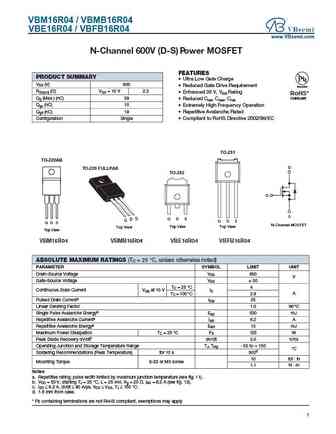
VBM16R04 / VBMB16R04 VBE16R04 / VBFB16R04 www.VBsemi.com N hannel 600 D S Power MOSFET FEATURES PRODUCT SUMMARY Ultra Low Gate Charge VDS (V) 600 Reduced Gate Drive Requirement Available RDS(on) ( )VGS = 10 V 2.2 Enhanced 30 V, VGS Rating RoHS* Qg (Max.) (nC) 39 COMPLIANT Reduced Ciss, Coss, Crss Qgs (nC) 10 Extremely High Frequency Operation Qgd (nC) ... See More ⇒
9.12. Size:605K cn vbsemi
vbfb1311.pdf 

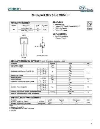
VBFB1311 www.VBsemi.com N-Channel 30-V (D-S) MOSFET FEATURES PRODUCT SUMMARY Halogen-free VDS (V) RDS(on) ( ) Qg (Typ.) ID (A) TrenchFET Gen III Power MOSFET 0.07 at VGS = 10 V 53 100 % Rg Tested RoHS 30 19 nC COMPLIANT 100 % UIS Tested 0.09 at VGS = 4.5 V 48 APPLICATIONS TO-251 DC/DC Conversion D - System Power G S N-Channel MOSFET G D S To... See More ⇒
9.13. Size:1462K cn vbsemi
vbm16r02 vbmb16r02 vbe16r02 vbfb16r02.pdf 

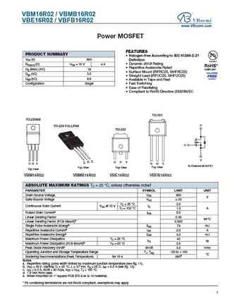
VBM16R02 / VBMB16R02 VBE16R02 / VBFB16R02 www.VBsemi.com Power MOSFET FEATURES PRODUCT SUMMARY Halogen-free According to IEC 61249-2-21 VDS (V) 600 Definition Dynamic dV/dt Rating RDS(on) ( )VGS = 10 V 4.4 Repetitive Avalanche Rated Qg (Max.) (nC) 18 Surface Mount (IRFRC20, SiHFRC20) Qgs (nC) 3.0 Straight Lead (IRFUC20, SiHFUC20) Qgd (nC) 8.9 Available ... See More ⇒
9.14. Size:881K cn vbsemi
vbfb1615.pdf 

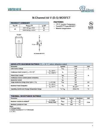
VBFB1615 www.VBsemi.com N-Channel 60 V (D-S) MOSFET FEATURES PRODUCT SUMMARY 175 C Junction Temperature VDS (V) RDS(on) ( ) ID (A)a TrenchFET Power MOSFET 0.011 at VGS = 10 V 55 Material categorization 60 0.012 at VGS = 4.5 V 47 TO-251 D G S N-Channel MOSFET G D S Top View ABSOLUTE MAXIMUM RATINGS (TC = 25 C, unless otherwise noted) Parameter Symbo... See More ⇒
9.15. Size:1415K cn vbsemi
vbfb165r02.pdf 

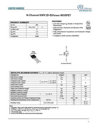
VBFB165R02 www.VBsemi.com N hannel 650 D S Power MOSFET FEATURES PRODUCT SUMMARY Low Gate Charge Qg Results in Simple Drive VDS (V) 650 Available Requirement RDS(on) ( )VGS = 10 V 5 RoHS Improved Gate, Avalanche and Dynamic dV/dt COMPLIANT Qg (Max.) (nC) 11 Ruggedness Qgs (nC) 2.3 Fully Characterized Capacitance and Avalanche Voltage and Current Qgd (nC) 5.... See More ⇒
Detailed specifications: VBE2509, VBE2610N, VBE2625, VBE2658, VBE3310, VBE5415, VBE5638, VBF2355, IRF1010E, VBFB1102M, VBFB1104N, VBFB1203M, VBFB1208N, VBFB1303, VBFB1311, VBFB1405, VBFB1410
Keywords - VBFB1101M MOSFET specs
VBFB1101M cross reference
VBFB1101M equivalent finder
VBFB1101M pdf lookup
VBFB1101M substitution
VBFB1101M replacement
Need a MOSFET replacement?
Our guide shows you how to find a perfect substitute by comparing key parameters and specs
