NCE3420 Datasheet. Specs and Replacement
Type Designator: NCE3420 📄📄
Type of Transistor: MOSFET
Type of Control Channel: N-Channel
Absolute Maximum Ratings
Pd ⓘ - Maximum Power Dissipation: 1.25 W
|Vds|ⓘ - Maximum Drain-Source Voltage: 20 V
|Vgs|ⓘ - Maximum Gate-Source Voltage: 10 V
|Id| ⓘ - Maximum Drain Current: 6 A
Tj ⓘ - Maximum Junction Temperature: 150 °C
Electrical Characteristics
tr ⓘ - Rise Time: 7.5 nS
Cossⓘ - Output Capacitance: 90 pF
RDSonⓘ - Maximum Drain-Source On-State Resistance: 0.028 Ohm
Package: SOT23
📄📄 Copy
- MOSFET ⓘ Cross-Reference Search
NCE3420 datasheet
..1. Size:246K ncepower
nce3420.pdf 
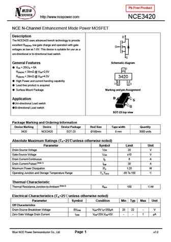
Pb Free Product http //www.ncepower.com NCE3420 NCE N-Channel Enhancement Mode Power MOSFET Description D The NCE3420 uses advanced trench technology to provide excellent RDS(ON), low gate charge and operation with gate G voltages as low as 1.8V. This device is suitable for use as a uni-directional or bi-directional load switch. S Schematic diagram General Features VD... See More ⇒
0.1. Size:318K ncepower
nce3420x.pdf
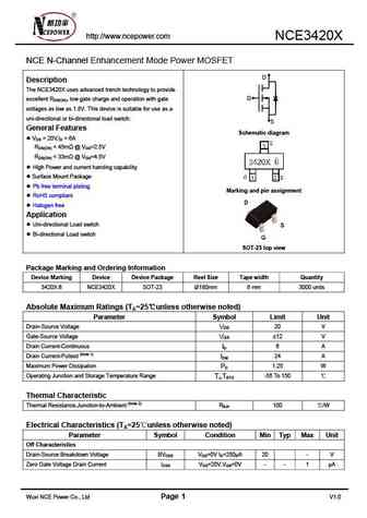
http //www.ncepower.com NCE3420X NCE N-Channel Enhancement Mode Power MOSFET D Description The NCE3420X uses advanced trench technology to provide G excellent RDS(ON), low gate charge and operation with gate voltages as low as 1.8V. This device is suitable for use as a uni-directional or bi-directional load switch. S General Features Schematic diagram VDS = 20V,ID = 6A... See More ⇒
9.1. Size:249K 1
nce3401ay.pdf
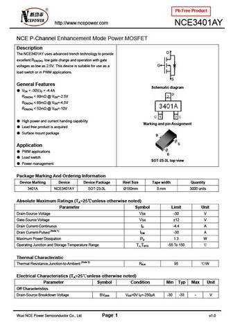
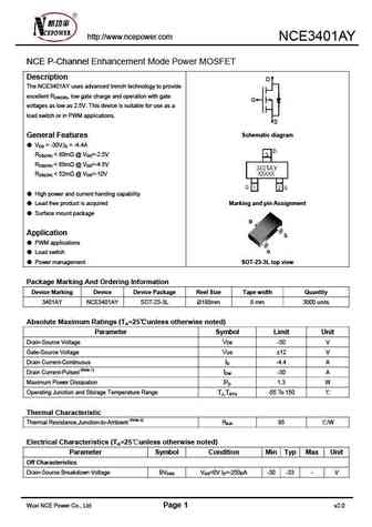
Pb Free Product http //www.ncepower.com NCE3401AY NCE P-Channel Enhancement Mode Power MOSFET Description D The NCE3401AY uses advanced trench technology to provide excellent RDS(ON), low gate charge and operation with gate G voltages as low as 2.5V. This device is suitable for use as a load switch or in PWM applications. S General Features Schematic diagram VDS = -30... See More ⇒
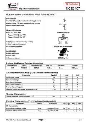
9.2. Size:602K ncepower
nce3407a.pdf
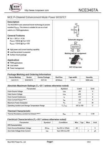
http //www.ncepower.com NCE3407A NCE P-Channel Enhancement Mode Power MOSFET Description D The NCE3407A uses advanced trench technology to provide excellent R , This device is suitable for use as a load DS(ON) G switch or in PWM applications. General Features S V = -30V,I = -4.3A DS D Schematic diagram R ... See More ⇒
9.3. Size:812K ncepower
nce3404x.pdf
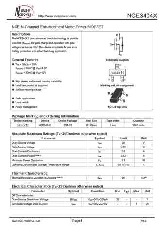
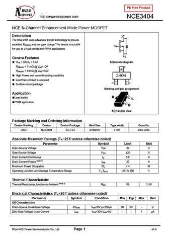
http //www.ncepower.com NCE3404X NCE N-Channel Enhancement Mode Power MOSFET Description D The NCE3404X uses advanced trench technology to provide excellent R , low gate charge and operation with gate DS(ON) G voltages as low as 4.5V. This device is suitable for use as a Battery protection or in other Switching application. S Schematic diagram General Features V = 30V,I = 5.8A... See More ⇒
9.4. Size:248K ncepower
nce3401a.pdf
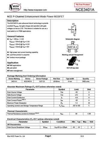
Pb Free Product http //www.ncepower.com NCE3401A NCE P-Channel Enhancement Mode Power MOSFET Description The NCE3401A uses advanced trench technology to provide D excellent RDS(ON), low gate charge and operation with gate voltages as low as 2.5V. This device is suitable for use as a G load switch or in PWM applications. S General Features VDS = -30V,ID = -4.4A Schematic... See More ⇒
9.5. Size:326K ncepower
nce3400.pdf

Pb Free Product http //www.ncepower.com NCE3400 NCE N-Channel Enhancement Mode Power MOSFET Description D The NCE3400 uses advanced trench technology to provide excellent RDS(ON), low gate charge and operation with gate G voltages as low as 2.5V. This device is suitable for use as a Battery protection or in other Switching application. S General Features Schematic diagram ... See More ⇒
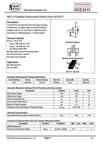
9.6. Size:263K ncepower
nce3415y.pdf
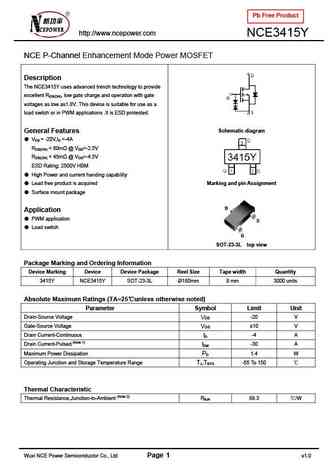
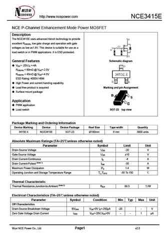
Pb Free Product http //www.ncepower.com NCE3415Y NCE P-Channel Enhancement Mode Power MOSFET Description The NCE3415Y uses advanced trench technology to provide excellent RDS(ON), low gate charge and operation with gate voltages as low as1.8V. This device is suitable for use as a load switch or in PWM applications .It is ESD protested. Schematic diagram General Features ... See More ⇒
9.7. Size:281K ncepower
nce3407.pdf
Pb Free Product http //www.ncepower.com NCE3407 NCE P-Channel Enhancement Mode Power MOSFET Description D The NCE3407 uses advanced trench technology to provide excellent RDS(ON), This device is suitable for use as a load G switch or in PWM applications. S General Features VDS = -30V,ID = -4.1A Schematic diagram RDS(ON) ... See More ⇒
9.8. Size:283K ncepower
nce3415.pdf
Pb Free Product http //www.ncepower.com NCE3415 NCE P-Channel Enhancement Mode Power MOSFET Description The NCE3415 uses advanced trench technology to provide excellent RDS(ON), low gate charge and operation with gate voltages as low as1.8V. This device is suitable for use as a load switch or in PWM applications .It is ESD protested. General Features VDS = -20V,ID =-4A S... See More ⇒
9.9. Size:278K ncepower
nce3400xy.pdf
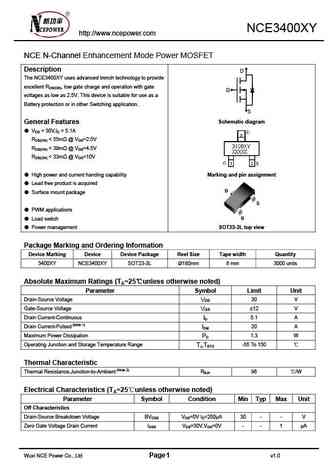
NCE3400XY http //www.ncepower.com NCE N-Channel Enhancement Mode Power MOSFET Description D The NCE3400XY uses advanced trench technology to provide excellent RDS(ON), low gate charge and operation with gate G voltages as low as 2.5V. This device is suitable for use as a Battery protection or in other Switching application. S Schematic diagram General Features VDS = 30... See More ⇒
9.10. Size:244K ncepower
nce3402a.pdf
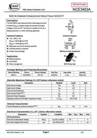
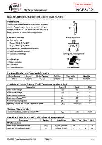
Pb Free Product http //www.ncepower.com NCE3402A NCE N-Channel Enhancement Mode Power MOSFET Description D The NCE3402A uses advanced trench technology to provide excellent RDS(ON), low gate charge and operation with gate G voltages as low as 2.5V. This device is suitable for use as a Battery protection or in other Switching application. S Schematic diagram General Features... See More ⇒
9.11. Size:271K ncepower
nce3406an.pdf
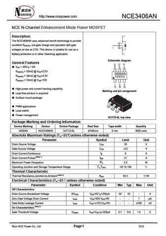
http //www.ncepower.com NCE3406AN NCE N-Channel Enhancement Mode Power MOSFET Description The NCE3406AN uses advanced trench technology to provide excellent RDS(ON), low gate charge and operation with gate voltages as low as 2.5V. This device is suitable for use as a Battery protection or in other Switching application. Schematic diagram General Features VDS = 30V,ID = 6A... See More ⇒
9.12. Size:298K ncepower
nce3400x.pdf

http //www.ncepower.com NCE3400X NCE N-Channel Enhancement Mode Power MOSFET Description D The NCE3400X uses advanced trench technology to provide excellent RDS(ON), low gate charge and operation with gate G voltages as low as 2.5V. This device is suitable for use as a Battery protection or in other Switching application. S General Features Schematic diagram VDS = 30V,... See More ⇒
9.13. Size:241K ncepower
nce3401.pdf
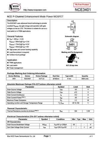
Pb Free Product http //www.ncepower.com NCE3401 NCE P-Channel Enhancement Mode Power MOSFET Description D The NCE3401 uses advanced trench technology to provide excellent RDS(ON), low gate charge and operation with gate G voltages as low as 2.5V. This device is suitable for use as a load switch or in PWM applications. S Schematic diagram General Features VDS = -30V,ID... See More ⇒
9.14. Size:247K ncepower
nce3400ay.pdf

http //www.ncepower.com NCE3400AY NCE N-Channel Enhancement Mode Power MOSFET Description D The NCE3400AY uses advanced trench technology to provide excellent RDS(ON), low gate charge and operation with gate G voltages as low as 2.5V. This device is suitable for use as a Battery protection or in other Switching application. S General Features Schematic diagram VDS = 30... See More ⇒
9.15. Size:265K ncepower
nce3401by.pdf
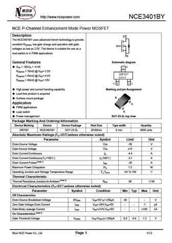
http //www.ncepower.com NCE3401BY NCE P-Channel Enhancement Mode Power MOSFET Description D The NCE3401BY uses advanced trench technology to provide excellent RDS(ON), low gate charge and operation with gate G voltages as low as 2.5V. This device is suitable for use as a load switch or in PWM applications. S Schematic diagram General Features VDS = -30V,ID = -4.4A RD... See More ⇒
9.16. Size:243K ncepower
nce3401y.pdf
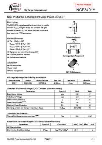
Pb Free Product http //www.ncepower.com NCE3401Y NCE P-Channel Enhancement Mode Power MOSFET D Description The NCE3401Y uses advanced trench technology to provide G excellent RDS(ON), low gate charge and operation with gate voltages as low as 2.5V. This device is suitable for use as a load switch or in PWM applications. S Schematic diagram General Features VDS = -30V,... See More ⇒
9.17. Size:267K ncepower
nce3401ay.pdf
http //www.ncepower.com NCE3401AY NCE P-Channel Enhancement Mode Power MOSFET Description D The NCE3401AY uses advanced trench technology to provide excellent RDS(ON), low gate charge and operation with gate G voltages as low as 2.5V. This device is suitable for use as a load switch or in PWM applications. S Schematic diagram General Features VDS = -30V,ID = -4.4A RD... See More ⇒
9.18. Size:238K ncepower
nce3400e.pdf
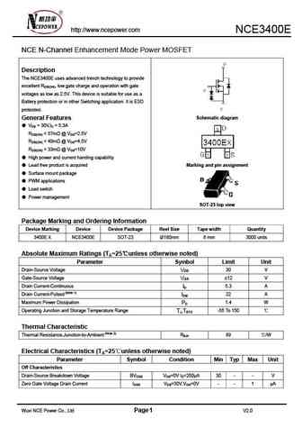
http //www.ncepower.com NCE3400E NCE N-Channel Enhancement Mode Power MOSFET Description The NCE3400E uses advanced trench technology to provide excellent RDS(ON), low gate charge and operation with gate voltages as low as 2.5V. This device is suitable for use as a Battery protection or in other Switching application. It is ESD protested. Schematic diagram General Features ... See More ⇒
9.19. Size:261K ncepower
nce3407ay.pdf
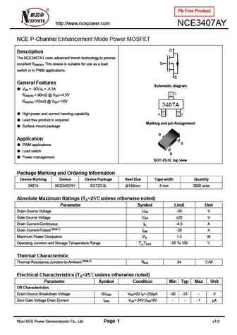
Pb Free Product http //www.ncepower.com NCE3407AY NCE P-Channel Enhancement Mode Power MOSFET D Description The NCE3407AY uses advanced trench technology to provide G excellent RDS(ON), This device is suitable for use as a load switch or in PWM applications. S General Features Schematic diagram VDS = -30V,ID = -4.3A RDS(ON) ... See More ⇒
9.20. Size:283K ncepower
nce3406n.pdf
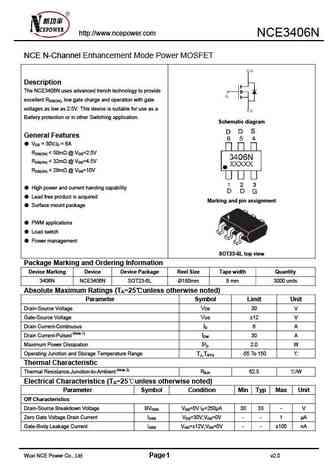
http //www.ncepower.com NCE3406N NCE N-Channel Enhancement Mode Power MOSFET Description The NCE3406N uses advanced trench technology to provide excellent RDS(ON), low gate charge and operation with gate voltages as low as 2.5V. This device is suitable for use as a Battery protection or in other Switching application. Schematic diagram General Features VDS = 30V,ID = 6A ... See More ⇒
9.21. Size:261K ncepower
nce3416.pdf
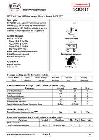
Pb Free Product http //www.ncepower.com NCE3416 NCE N-Channel Enhancement Mode Power MOSFET Description The NCE3416 uses advanced trench technology to provide excellent RDS(ON), low gate charge and operation with gate voltages as low as 1.8V. This device is suitable for use as a load switch or in PWM applications .It is ESD protested. General Features VDS = 20V,ID =6.5A Sc... See More ⇒
9.22. Size:272K ncepower
nce3417.pdf
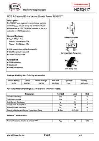
Pb Free Product http //www.ncepower.com NCE3417 NCE P-Channel Enhancement Mode Power MOSFET Description D The NCE3417 uses advanced trench technology to provide excellent RDS(ON), low gate charge and operation with gate G voltages as low as 2.5V. This device is suitable for use as a load switch or in PWM applications. S General Features Schematic diagram VDS = -12V,ID... See More ⇒
9.23. Size:253K ncepower
nce3404y.pdf
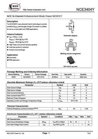
http //www.ncepower.com NCE3404Y NCE N-Channel Enhancement Mode Power MOSFET D Description The NCE3404Y uses advanced trench technology to provide G excellent RDS(ON) and low gate charge.This device is suitable for use as a load switch and PWM applications. S Genera Features Schematic diagram VDS = 30V,ID = 5.8A RDS(ON) ... See More ⇒
9.24. Size:615K ncepower
nce3401e.pdf
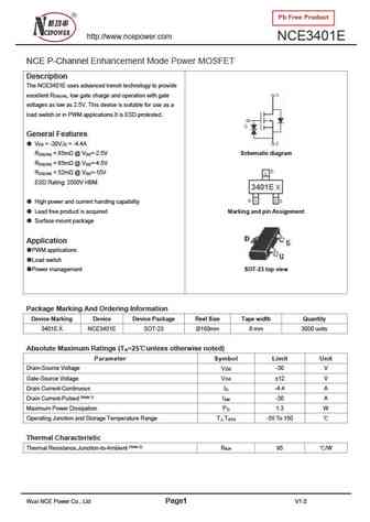
Pb Free Product http //www.ncepower.com NCE3401E NCE P-Channel Enhancement Mode Power MOSFET Description The NCE3401E uses advanced trench technology to provide excellent R , low gate charge and operation with gate DS(ON) voltages as low as 2.5V. This device is suitable for use as a load switch or in PWM applications.It is ESD protested. General Features V = -30V,I = -4.4A DS D ... See More ⇒
9.25. Size:241K ncepower
nce3402.pdf
Pb Free Product http //www.ncepower.com NCE3402 NCE N-Channel Enhancement Mode Power MOSFET Description D The NCE3402 uses advanced trench technology to provide excellent RDS(ON), low gate charge and operation with gate G voltages as low as 2.5V. This device is suitable for use as a Battery protection or in other Switching application. S Schematic diagram General Features ... See More ⇒
9.26. Size:242K ncepower
nce3415e.pdf
http //www.ncepower.com NCE3415E NCE P-Channel Enhancement Mode Power MOSFET Description The NCE3415E uses advanced trench technology to provide excellent RDS(ON), low gate charge and operation with gate voltages as low as1.8V. This device is suitable for use as a load switch or in PWM applications .It is ESD protested. Schematic diagram General Features VDS = -20V,ID =-4... See More ⇒
9.27. Size:729K ncepower
nce3407e.pdf
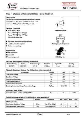
Pb Free Product http //www.ncepower.com NCE3407E NCE P-Channel Enhancement Mode Power MOSFET Description The NCE3407E uses advanced trench technology to provide excellent R . This device is suitable for use as a load DS(ON) switch or in PWM applications.It is ESD protected. General Features V = -30V,I = -4.3A Schematic diagram DS D R = 28m @ V =-10V (typ) DS(ON) GS R = 38m ... See More ⇒
9.29. Size:248K ncepower
nce3400a.pdf
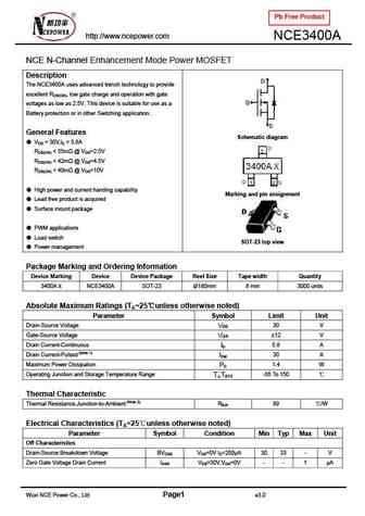
Pb Free Product http //www.ncepower.com NCE3400A NCE N-Channel Enhancement Mode Power MOSFET Description D The NCE3400A uses advanced trench technology to provide excellent RDS(ON), low gate charge and operation with gate G voltages as low as 2.5V. This device is suitable for use as a Battery protection or in other Switching application. S General Features Schematic diagram... See More ⇒
9.30. Size:895K cn vbsemi
nce3404.pdf
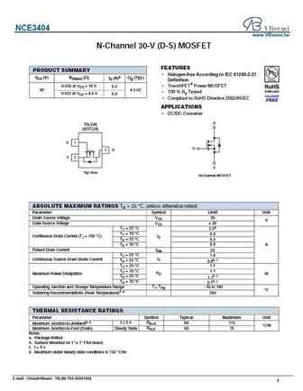
NCE3404 www.VBsemi.tw N-Channel 30-V (D-S) MOSFET FEATURES PRODUCT SUMMARY Halogen-free According to IEC 61249-2-21 VDS (V) RDS(on) ( ) ID (A)a Qg (Typ.) Definition 0.030 at VGS = 10 V TrenchFET Power MOSFET 6.5 30 4.5 nC 100 % Rg Tested 0.033 at VGS = 4.5 V 6.0 Compliant to RoHS Directive 2002/95/EC APPLICATIONS DC/DC Converter D TO-236 (SOT-23) G ... See More ⇒
9.31. Size:848K cn vbsemi
nce3400a.pdf

NCE3400A www.VBsemi.tw N-Channel 30-V (D-S) MOSFET FEATURES PRODUCT SUMMARY Halogen-free According to IEC 61249-2-21 VDS (V) RDS(on) ( ) ID (A)a Qg (Typ.) Definition 0.030 at VGS = 10 V TrenchFET Power MOSFET 6.5 30 4.5 nC 100 % Rg Tested 0.033 at VGS = 4.5 V 6.0 Compliant to RoHS Directive 2002/95/EC APPLICATIONS DC/DC Converter D TO-236 (SOT-23) G... See More ⇒
Detailed specifications: NCE3400X, NCE3401, NCE3404Y, NCE3406N, NCE3407, NCE3407AY, NCE3415, NCE3416, IRF640, NCE4009S, NCE4012S, NCE4060I, NCE4060K, NCE4080, NCE4080D, NCE4080K, NCE40H12
Keywords - NCE3420 MOSFET specs
NCE3420 cross reference
NCE3420 equivalent finder
NCE3420 pdf lookup
NCE3420 substitution
NCE3420 replacement
Can't find your MOSFET?
Learn how to find a substitute transistor by analyzing voltage, current and package compatibility