NCEP039N10MD Specs and Replacement
Type Designator: NCEP039N10MD
Type of Transistor: MOSFET
Type of Control Channel: N-Channel
Absolute Maximum Ratings
Pd ⓘ - Maximum Power Dissipation: 220 W
|Vds|ⓘ - Maximum Drain-Source Voltage: 100 V
|Vgs|ⓘ - Maximum Gate-Source Voltage: 20 V
|Id| ⓘ - Maximum Drain Current: 135 A
Tj ⓘ - Maximum Junction Temperature: 175 °C
Electrical Characteristics
tr ⓘ - Rise Time: 11.5 nS
Cossⓘ - Output Capacitance: 618 pF
RDSonⓘ - Maximum Drain-Source On-State Resistance: 0.0039 Ohm
Package: TO263
NCEP039N10MD substitution
- MOSFET ⓘ Cross-Reference Search
NCEP039N10MD datasheet
ncep039n10md.pdf

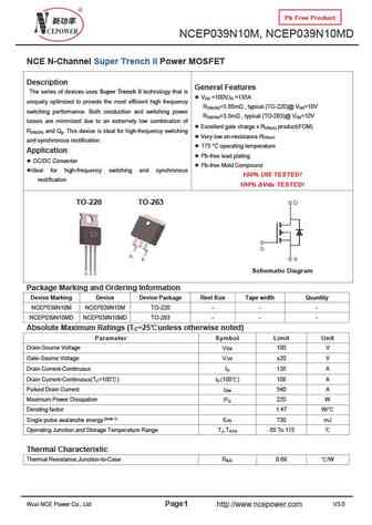
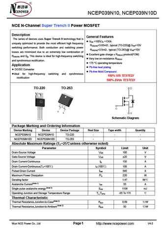
Pb Free Product NCEP039N10M, NCEP039N10MD NCE N-Channel Super Trench II Power MOSFET Description General Features The series of devices uses Super Trench II technology that is V =100V,I =135A DS D uniquely optimized to provide the most efficient high frequency R =3.65m , typical (TO-220)@ V =10V DS(ON) GS switching performance. Both conduction and switching power R =3.5m , t... See More ⇒
ncep039n10m ncep039n10md.pdf
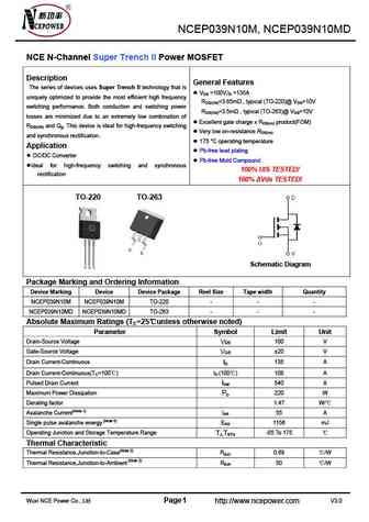
NCEP039N10M, NCEP039N10MD NCE N-Channel Super Trench II Power MOSFET Description General Features The series of devices uses Super Trench II technology that is VDS =100V,ID =135A uniquely optimized to provide the most efficient high frequency RDS(ON)=3.65m , typical (TO-220)@ VGS=10V switching performance. Both conduction and switching power RDS(ON)=3.5m , typical (... See More ⇒
ncep039n10m.pdf
Pb Free Product NCEP039N10M, NCEP039N10MD NCE N-Channel Super Trench II Power MOSFET Description General Features The series of devices uses Super Trench II technology that is V =100V,I =135A DS D uniquely optimized to provide the most efficient high frequency R =3.65m , typical (TO-220)@ V =10V DS(ON) GS switching performance. Both conduction and switching power R =3.5m , t... See More ⇒
ncep039n10d.pdf

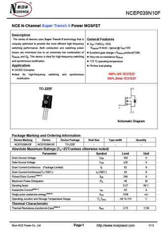
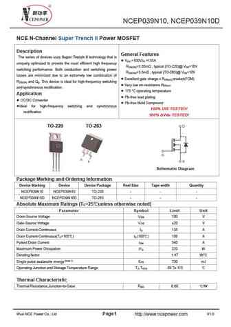
NCEP039N10, NCEP039N10D NCE N-Channel Super Trench II Power MOSFET Description General Features The series of devices uses Super Trench II technology that is V =100V,I =135A DS D uniquely optimized to provide the most efficient high frequency R =3.65m , typical (TO-220)@ V =10V DS(ON) GS switching performance. Both conduction and switching power R =3.5m , typical (TO-263)@ V ... See More ⇒
Detailed specifications: NCEP028N85D, NCEP02T10D, NCEP033N85, NCEP033N85D, NCEP035N85GU, NCEP039N10, NCEP039N10D, NCEP039N10M, IRF9540N, NCEP040N10, NCEP040N10D, NCEP040N85, NCEP040N85D, NCEP045N10, NCEP045N10D, NCEP050N85, NCEP050N85D
Keywords - NCEP039N10MD MOSFET specs
NCEP039N10MD cross reference
NCEP039N10MD equivalent finder
NCEP039N10MD pdf lookup
NCEP039N10MD substitution
NCEP039N10MD replacement
Need a MOSFET replacement? Our guide shows you how to find a perfect substitute by comparing key parameters and specs
🌐 : EN ES РУ

LIST
Last Update
MOSFET: AUN084N10 | AUN065N10 | AUN063N10 | AUN062N08BG | AUN060N08AG | AUN053N10 | AUN050N08BGL | AUN045N085 | AUN042N055 | AUN036N10
Popular searches
p157r5nt | ptp03n04n | sm4377 mosfet datasheet | tip31c reemplazo | 2sa906 | c2389 transistor | c2634 transistor | mdp1991 datasheet