SW3N90U Specs and Replacement
Type Designator: SW3N90U
Type of Transistor: MOSFET
Type of Control Channel: N-Channel
Absolute Maximum Ratings
Pd ⓘ - Maximum Power Dissipation: 178.6 W
|Vds|ⓘ - Maximum Drain-Source Voltage: 900 V
|Vgs|ⓘ - Maximum Gate-Source Voltage: 30 V
|Id| ⓘ - Maximum Drain Current: 3 A
Tj ⓘ - Maximum Junction Temperature: 150 °C
Electrical Characteristics
tr ⓘ - Rise Time: 24 nS
Cossⓘ - Output Capacitance: 49 pF
RDSonⓘ - Maximum Drain-Source On-State Resistance: 5.8 Ohm
Package: TO251
SW3N90U substitution
- MOSFET ⓘ Cross-Reference Search
SW3N90U datasheet
sw3n90u swi3n90u swmi3n90u swd3n90u.pdf
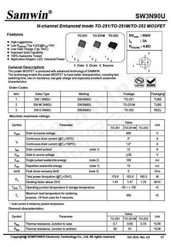
SW3N90U N-channel Enhanced mode TO-251/TO-251M/TO-252 MOSFET Features TO-251 TO-251M TO-252 BVDSS 900V ID 3A High ruggedness Low RDS(ON) (Typ 4.8 )@VGS=10V RDS(ON) 4.8 Low Gate Charge (Typ 19nC) Improved dv/dt Capability 2 100% Avalanche Tested 1 1 1 2 2 2 Application Adaptor, LED, Industrial Power 3 3 3 1. Gate 2. Drain 3. Sou... See More ⇒
sw3n90u.pdf
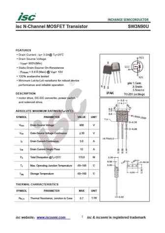
isc N-Channel MOSFET Transistor SW3N90U FEATURES Drain Current I = 3.0A@ T =25 D C Drain Source Voltage V = 900V(Min) DSS Static Drain-Source On-Resistance R = 5.8 (Max) @ V = 10V DS(on) GS 100% avalanche tested Minimum Lot-to-Lot variations for robust device performance and reliable operation DESCRIPTION motor drive, DC-DC converter, power switch and soleno... See More ⇒
ssw3n90a.pdf
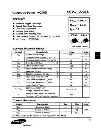
Advanced Power MOSFET FEATURES BVDSS = 900 V Avalanche Rugged Technology RDS(on) = 6.2 Rugged Gate Oxide Technology Lower Input Capacitance ID = 3 A Improved Gate Charge Extended Safe Operating Area Lower Leakage Current 25 A (Max.) @ VDS = 900V 2 Low RDS(ON) 4.679 (Typ.) 1 1 2 3 3 1. Gate 2. Drain 3. Source Absolute Maximum Ratings Symbol Charact... See More ⇒
Detailed specifications: ISF40NF20, ISH3N150, IXFY26N30X3, IXFA26N30X3, IXFP26N30X3, MMD60R900QRH, STF23N80K5, STF6N90K5, STP65NF06, SWI3N90U, SWMI3N90U, SWD3N90U, SCT10N120, SCT20N120, STB100N6F7, STB10LN80K5, STB15N65M5
Keywords - SW3N90U MOSFET specs
SW3N90U cross reference
SW3N90U equivalent finder
SW3N90U pdf lookup
SW3N90U substitution
SW3N90U replacement
Learn how to find the right MOSFET substitute. A guide to cross-reference, check specs and replace MOSFETs in your circuits.
History: ELM322806A | S40N09S
🌐 : EN ES РУ

LIST
Last Update
MOSFET: AUB062N08BG | AUB060N08AG | AUB056N10 | AUB056N08BGL | AUB050N085 | AUB050N055 | AUB045N12 | AUB045N10BT | AUB039N10 | AUB034N10
Popular searches
2sc828 | 2n4125 | tip42c transistor | c1815 transistor datasheet | mj15003 | 2sa1015 | ksc3503 | c945 transistor datasheet