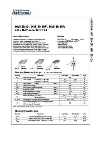
HM18N40F Specs and Replacement
Type Designator: HM18N40F
Type of Transistor: MOSFET
Type of Control Channel: N-Channel
Absolute Maximum Ratings
Pd ⓘ - Maximum Power Dissipation: 40 W
|Vds|ⓘ - Maximum Drain-Source Voltage: 400 V
|Vgs|ⓘ - Maximum Gate-Source Voltage: 30 V
|Id| ⓘ - Maximum Drain Current: 18 A
Tj ⓘ - Maximum Junction Temperature: 150 °C
Electrical Characteristics
tr ⓘ - Rise Time: 170 nS
Cossⓘ - Output Capacitance: 255 pF
RDSonⓘ - Maximum Drain-Source On-State Resistance: 0.25 Ohm
Package: TO3P
HM18N40F substitution
- MOSFET ⓘ Cross-Reference Search
HM18N40F datasheet
hm18n40 hm18n40f hm18n40a.pdf
HM18N40 / HM18N40F / HM18N40A 400V N-Channel MOSFET General Description Features This Power MOSFET is produced using Maple semi s - 18A, 400V, RDS(on) typ. = 0.20 @VGS = 10 V advanced planar stripe DMOS technology. - Low gate charge ( typical 50nC) This advanced technology has been especially tailored - High ruggedness to minimize on-state resistance, provide superior switching - Fast ... See More ⇒
phm18nq15t.pdf
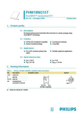
PHM18NQ15T TrenchMOS standard level FET Rev. 02 20 August 2004 Product data M3D879 1. Product profile 1.1 Description N-channel enhancement mode field-effect transistor in a plastic package using TrenchMOS technology. 1.2 Features SOT96 (SO-8) footprint compatible Low thermal resistance Surface mounted package Low profile. 1.3 Applications DC-to-DC converter primary sid... See More ⇒
hm18n50a hm18n50f.pdf
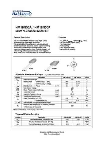
HM18N50A / HM18N50F 500V N-Channel MOSFET General Description Features This Power MOSFET is produced using Maple semi s - 18A, 500V, RDS(on)typ. = 236m @VGS = 10 V advanced planar stripe DMOS technology. - Low gate charge ( typical 69nC) This advanced technology has been especially tailored - High ruggedness to minimize on-state resistance, provide superior switching - Fast switching ... See More ⇒
hm18n03d.pdf
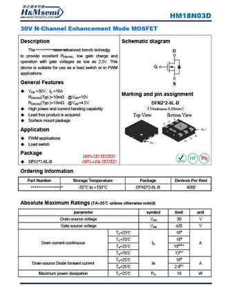
HM18N03D 30V N-Channel Enhancement Mode MOSFET Description Schematic diagram The uses advanced trench technol ogy D to provide excellent RDS(ON), low gate charge and operation with gate voltages as low as 2.5V. This G device is suitable for use as a load switch or in PWM applications. General Features S VDS =30V ID =18A Marking and pin assignment RDS(ON)(T... See More ⇒
Detailed specifications: HM17N10K, HM180N02, HM180N02D, HM180N02K, HM18DN03Q, HM18N03D, HM18N40, HM18N40A, 5N65, HM18N50A, HM18N50F, HM18P10, HM18P10K, HM19N40, HM1N50MR, HM1N60, HM1N60PR
Keywords - HM18N40F MOSFET specs
HM18N40F cross reference
HM18N40F equivalent finder
HM18N40F pdf lookup
HM18N40F substitution
HM18N40F replacement
Can't find your MOSFET? Learn how to find a substitute transistor by analyzing voltage, current and package compatibility
History: 2SK3130
🌐 : EN ES РУ
LIST
Last Update
MOSFET: AUB062N08BG | AUB060N08AG | AUB056N10 | AUB056N08BGL | AUB050N085 | AUB050N055 | AUB045N12 | AUB045N10BT | AUB039N10 | AUB034N10
Popular searches
c5242 reemplazo | d667 transistor datasheet | hy1d datasheet | mp20a transistor | mrf450 | oc70 transistor | p0603bd mosfet | p157r5nt


