HM18N40F. Аналоги и основные параметры
Наименование производителя: HM18N40F
Тип транзистора: MOSFET
Полярность: N
Предельные значения
Pd ⓘ - Максимальная рассеиваемая мощность: 40 W
|Vds|ⓘ - Максимально допустимое напряжение сток-исток: 400 V
|Vgs|ⓘ - Максимально допустимое напряжение затвор-исток: 30 V
|Id| ⓘ - Максимально допустимый постоянный ток стока: 18 A
Tj ⓘ - Максимальная температура канала: 150 °C
Электрические характеристики
tr ⓘ - Время нарастания: 170 ns
Cossⓘ - Выходная емкость: 255 pf
RDSonⓘ - Сопротивление сток-исток открытого транзистора: 0.25 Ohm
Тип корпуса: TO3P
Аналог (замена) для HM18N40F
- подборⓘ MOSFET транзистора по параметрам
HM18N40F даташит
hm18n40 hm18n40f hm18n40a.pdf
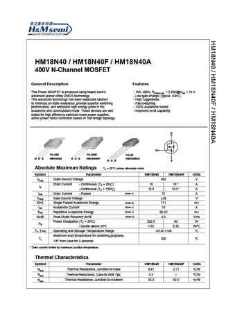
HM18N40 / HM18N40F / HM18N40A 400V N-Channel MOSFET General Description Features This Power MOSFET is produced using Maple semi s - 18A, 400V, RDS(on) typ. = 0.20 @VGS = 10 V advanced planar stripe DMOS technology. - Low gate charge ( typical 50nC) This advanced technology has been especially tailored - High ruggedness to minimize on-state resistance, provide superior switching - Fast
phm18nq15t.pdf
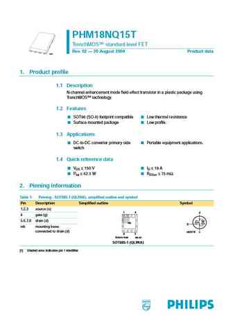
PHM18NQ15T TrenchMOS standard level FET Rev. 02 20 August 2004 Product data M3D879 1. Product profile 1.1 Description N-channel enhancement mode field-effect transistor in a plastic package using TrenchMOS technology. 1.2 Features SOT96 (SO-8) footprint compatible Low thermal resistance Surface mounted package Low profile. 1.3 Applications DC-to-DC converter primary sid
hm18n50a hm18n50f.pdf
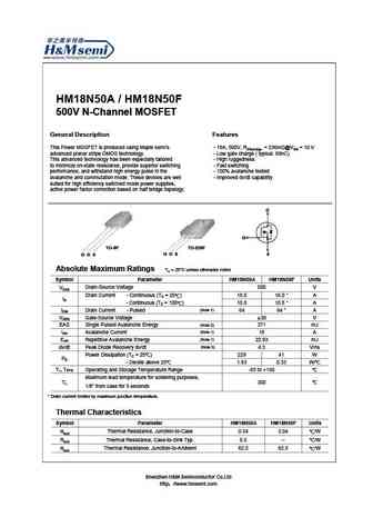
HM18N50A / HM18N50F 500V N-Channel MOSFET General Description Features This Power MOSFET is produced using Maple semi s - 18A, 500V, RDS(on)typ. = 236m @VGS = 10 V advanced planar stripe DMOS technology. - Low gate charge ( typical 69nC) This advanced technology has been especially tailored - High ruggedness to minimize on-state resistance, provide superior switching - Fast switching
hm18n03d.pdf
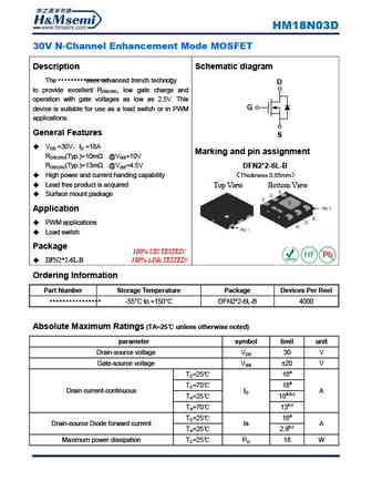
HM18N03D 30V N-Channel Enhancement Mode MOSFET Description Schematic diagram The uses advanced trench technol ogy D to provide excellent RDS(ON), low gate charge and operation with gate voltages as low as 2.5V. This G device is suitable for use as a load switch or in PWM applications. General Features S VDS =30V ID =18A Marking and pin assignment RDS(ON)(T
Другие MOSFET... HM17N10K , HM180N02 , HM180N02D , HM180N02K , HM18DN03Q , HM18N03D , HM18N40 , HM18N40A , 5N65 , HM18N50A , HM18N50F , HM18P10 , HM18P10K , HM19N40 , HM1N50MR , HM1N60 , HM1N60PR .
History: SI3429EDV | JMSL0303TU
History: SI3429EDV | JMSL0303TU
🌐 : EN ES РУ

Список транзисторов
Обновления
MOSFET: AUB062N08BG | AUB060N08AG | AUB056N10 | AUB056N08BGL | AUB050N085 | AUB050N055 | AUB045N12 | AUB045N10BT | AUB039N10 | AUB034N10 | AUB033N08BG | AUB026N085 | AUA062N08BG | AUA060N08AG | AUA056N08BGL | AUA039N10
Popular searches
c5242 reemplazo | d667 transistor datasheet | hy1d datasheet | mp20a transistor | mrf450 | oc70 transistor | p0603bd mosfet | p157r5nt