HM2301BKR Specs and Replacement
Type Designator: HM2301BKR
Type of Transistor: MOSFET
Type of Control Channel: P-Channel
Absolute Maximum Ratings
Pd ⓘ - Maximum Power Dissipation: 0.3 W
|Vds|ⓘ - Maximum Drain-Source Voltage: 20 V
|Vgs|ⓘ - Maximum Gate-Source Voltage: 6 V
|Id| ⓘ - Maximum Drain Current: 0.8 A
Electrical Characteristics
tr ⓘ - Rise Time: 24.2 nS
Cossⓘ - Output Capacitance: 18.5 pF
RDSonⓘ - Maximum Drain-Source On-State Resistance: 0.48 Ohm
Package: SOT323
HM2301BKR substitution
- MOSFET ⓘ Cross-Reference Search
HM2301BKR datasheet
hm2301bkr.pdf
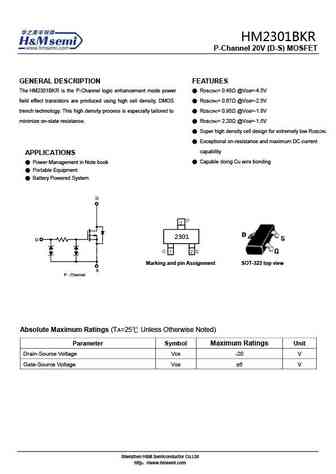
HM2301BKR P-Channel 20V (D-S) MOSFET GENERAL DESCRIPTION FEATURES The HM2301BKR is the P-Channel logic enhancement mode power RDS(ON)= 0.48 @VGS=-4.5V field effect transistors are produced using high cell density, DMOS RDS(ON)= 0.67 @VGS=-2.5V trench technology. This high density process is especially tailored to RDS(ON)= 0.95 @VGS=-1.8V minimize on-state resist... See More ⇒
hm2301bsr.pdf

HM2301BSR P-Channel 20V (D-S) MOSFET GENERAL DESCRIPTION FEATURES The HM2301BSR is the P-Channel logic enhancement mode power RDS(ON)= 0.48 @VGS=-4.5V field effect transistors are produced using high cell density, DMOS RDS(ON)= 0.67 @VGS=-2.5V trench technology. This high density process is especially tailored to RDS(ON)= 0.95 @VGS=-1.8V minimize on-state resist... See More ⇒
hm2301b.pdf
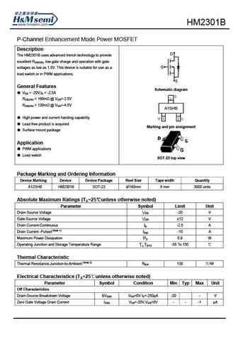
HM2301B P-Channel Enhancement Mode Power MOSFET Description D The HM2301B uses advanced trench technology to provide excellent RDS(ON), low gate charge and operation with gate G voltages as low as 1.8V. This device is suitable for use as a load switch or in PWM applications. S General Features Schematic diagram VDS = -20V,ID = -2.5A RDS(ON) ... See More ⇒
hm2301bjr.pdf
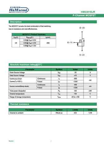
HM2301BJR P-Channel MOSFET Description The MOSFET provide the best combination of fast switching, D 3 low on-resistance and cost-effectiveness. MOSFET Product Summary V (V) R ( ) I (mA) DS DS(on) D 0.45@ V =-4.5V GS G 1 -20 0.62@ VGS=-2.5V -800 0.86@ V =-1.8V GS S 2 Absolute maximum rating@25 Parameter Symbol Value Units Drain-Source Voltage ... See More ⇒
Detailed specifications: HM2300C, HM2300D, HM2300DR, HM2300PR, HM2301, HM2301A, HM2301B, HM2301BJR, IRF9640, HM2301BSR, HM2301C, HM2301D, HM2301DR, HM2301E, HM2301F, HM2302, HM2302A
Keywords - HM2301BKR MOSFET specs
HM2301BKR cross reference
HM2301BKR equivalent finder
HM2301BKR pdf lookup
HM2301BKR substitution
HM2301BKR replacement
Step-by-step guide to finding a MOSFET replacement. Cross-reference parts and ensure compatibility for your repair or project.
History: LSGE085R041W3 | 2SK1001 | 2SK066500L
🌐 : EN ES РУ

LIST
Last Update
MOSFET: AUN084N10 | AUN065N10 | AUN063N10 | AUN062N08BG | AUN060N08AG | AUN053N10 | AUN050N08BGL | AUN045N085 | AUN042N055 | AUN036N10
Popular searches
2n4401 datasheet | irf640 | irf840 | irf740 | c945 transistor | irf640n | 2n3904 | bc547 datasheet