HM2309AL Specs and Replacement
Type Designator: HM2309AL
Type of Transistor: MOSFET
Type of Control Channel: P-Channel
Absolute Maximum Ratings
Pd ⓘ - Maximum Power Dissipation: 1.5 W
|Vds|ⓘ - Maximum Drain-Source Voltage: 60 V
|Vgs|ⓘ - Maximum Gate-Source Voltage: 20 V
|Id| ⓘ - Maximum Drain Current: 4.6 A
Tj ⓘ - Maximum Junction Temperature: 150 °C
Electrical Characteristics
tr ⓘ - Rise Time: 4 nS
Cossⓘ - Output Capacitance: 85 pF
RDSonⓘ - Maximum Drain-Source On-State Resistance: 0.075 Ohm
Package: SOT23
HM2309AL substitution
- MOSFET ⓘ Cross-Reference Search
HM2309AL datasheet
hm2309al.pdf
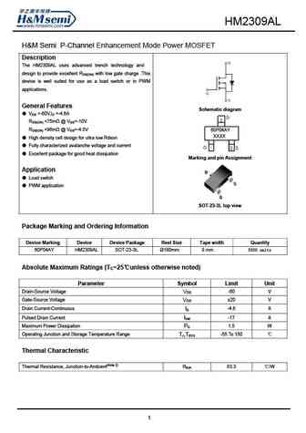
HM2309AL H&M Semi P-Channel Enhancement Mode Power MOSFET Description The HM2309AL uses advanced trench technology and design to provide excellent RDS(ON) with low gate charge .This device is well suited for use as a load switch or in PWM applications. General Features Schematic diagram VDS =-60V,ID =-4.6A RDS(ON) ... See More ⇒
hm2309apr.pdf
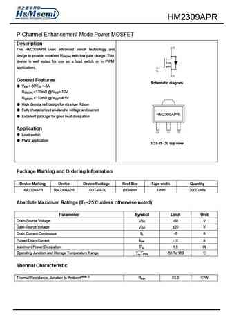
HM2309APR P-Channel Enhancement Mode Power MOSFET Description The HM2309APR uses advanced trench technology and design to provide excellent RDS(ON) with low gate charge .This device is well suited for use as a load switch or in PWM applications. General Features Schematic diagram VDS =-60V,ID =-5A RDS(ON) ... See More ⇒
hm2309.pdf
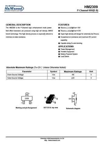
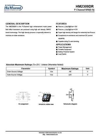
HM2309 P-Channel 60V(D-S) GENERAL DESCRIPTION FEATURES RDS(ON) 215m @VGS=-10V The HM2309 is the P-Channel logic enhancement mode power RDS(ON) 260m @VGS=-4.5V field effect transistors are produced using high cell density, DMOS Super high density cell design for extremely low RDS(ON) trench technology. This high density process is especially tailored to Ex... See More ⇒
hm2309b.pdf
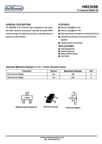
HM2309B P-Channel 60V(D-S) GENERAL DESCRIPTION FEATURES RDS(ON) 188m @VGS=-10V The HM2309B is the P-Channel logic enhancement mode power RDS(ON) 266m @VGS=-4.5V field effect transistors are produced using high cell density, DMOS Super high density cell design for extremely low RDS(ON) trench technology. This high density process is especially tailored to ... See More ⇒
Detailed specifications: HM2302E, HM2302F, HM2302KR, HM2305, HM2305B, HM2305D, HM2306, HM2309, IRF640, HM2309APR, HM2309B, HM2309C, HM2309D, HM2309DR, HM2310B, HM2310C, HM2312
Keywords - HM2309AL MOSFET specs
HM2309AL cross reference
HM2309AL equivalent finder
HM2309AL pdf lookup
HM2309AL substitution
HM2309AL replacement
Can't find your MOSFET? Learn how to find a substitute transistor by analyzing voltage, current and package compatibility
🌐 : EN ES РУ

LIST
Last Update
MOSFET: AUN084N10 | AUN065N10 | AUN063N10 | AUN062N08BG | AUN060N08AG | AUN053N10 | AUN050N08BGL | AUN045N085 | AUN042N055 | AUN036N10
Popular searches
2n3055 | irfp260n | 2n2222 datasheet | irf9540 | 2n3055 datasheet | 2sc945 | irfp250n | irf9540n