HM3407A Specs and Replacement
Type Designator: HM3407A
Type of Transistor: MOSFET
Type of Control Channel: P-Channel
Absolute Maximum Ratings
Pd ⓘ
- Maximum Power Dissipation: 1.4 W
|Vds|ⓘ - Maximum Drain-Source Voltage: 30 V
|Vgs|ⓘ - Maximum Gate-Source Voltage: 20 V
|Id| ⓘ - Maximum Drain Current: 4.1 A
Tj ⓘ - Maximum Junction Temperature: 150 °C
Electrical Characteristics
tr ⓘ - Rise Time: 5 nS
Cossⓘ -
Output Capacitance: 120 pF
RDSonⓘ - Maximum Drain-Source On-State Resistance: 0.06 Ohm
Package: SOT23
- MOSFET ⓘ Cross-Reference Search
HM3407A datasheet
..1. Size:526K cn hmsemi
hm3407a.pdf 
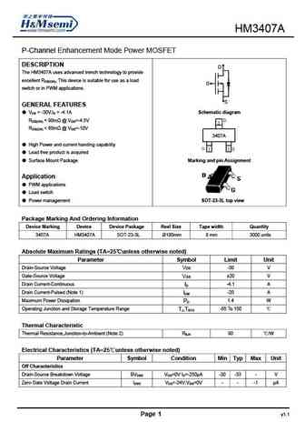
HM3407A P-Channel Enhancement Mode Power MOSFET DESCRIPTION D The HM3407A uses advanced trench technology to provide excellent RDS(ON), This device is suitable for use as a load G switch or in PWM applications. S GENERAL FEATURES VDS = -30V,ID = -4.1A Schematic diagram RDS(ON) ... See More ⇒
8.1. Size:460K cn hmsemi
hm3407b.pdf
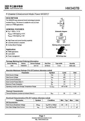
HM3407B P-Channel Enhancement Mode Power MOSFET DESCRIPTION D The HM3407B uses advanced trench technology to provide excellent RDS(ON), This device is suitable for use as a load G switch or in PWM applications. S GENERAL FEATURES VDS = -30V,ID = -4.1A Schematic diagram RDS(ON) ... See More ⇒
9.1. Size:1663K cn vbsemi
hm3400pr.pdf
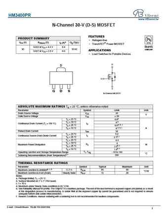
HM3400PR www.VBsemi.tw N-Channel 30-V (D-S) MOSFET FEATURES PRODUCT SUMMARY Halogen-free VDS (V) RDS(on) ( ) ID (A)a Qg (Typ.) TrenchFET Power MOSFET 0.022 at VGS = 4.5 V 6.8 RoHS 30 10 nC COMPLIANT APPLICATIONS 0.027 at VGS = 2.5 V 6.0 Load Switches for Portable Devices D D G S G D S N-Channel MOSFET ABSOLUTE MAXIMUM RATINGS TA = 25 C, unless otherwise n... See More ⇒
9.2. Size:547K cn hmsemi
hm3401.pdf
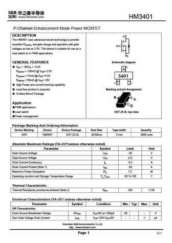
HM3401 P-Channel Enhancement Mode Power MOSFET DESCRIPTION D The HM3401 uses advanced trench technology to provide excellent RDS(ON), low gate charge and operation with gate G voltages as low as 2.5V. This device is suitable for use as a load switch or in PWM applications. S Schematic diagram GENERAL FEATURES VDS = -30V,ID = -4.2A RDS(ON) ... See More ⇒
9.3. Size:588K cn hmsemi
hm3401d.pdf
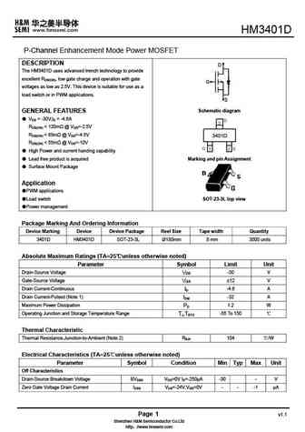
HM3401 P-Channel Enhancement Mode Power MOSFET DESCRIPTION D The HM3401 uses advanced trench technology to provide excellent RDS(ON), low gate charge and operation with gate G voltages as low as 2.5V. This device is suitable for use as a load switch or in PWM applications. S Schematic diagram GENERAL FEATURES VDS = -30V,ID = -4.6A RDS(ON) ... See More ⇒
9.4. Size:384K cn hmsemi
hm3400 sot23-3l.pdf

HM3400 N-Channel Enhancement Mode Power MOSFET DESCRIPTION The HM3400 uses advanced trench technology to provide D excellent RDS(ON), low gate charge and operation with gate voltages as low as 2.5V. This device is suitable for use as a G Battery protection or in other Switching application. S GENERAL FEATURES VDS = 30V,ID = 5.8A Schematic diagram RDS(ON) ... See More ⇒
9.5. Size:560K cn hmsemi
hm3401c.pdf
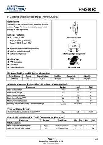
HM3401C P-Channel Enhancement Mode Power MOSFET Description D The HM3401C uses advanced trench technology to provide excellent RDS(ON), This device is suitable for use as a load G switch or in PWM applications. S General Features VDS = -30V,ID = -2.5A Schematic diagram RDS(ON) ... See More ⇒
9.6. Size:478K cn hmsemi
hm3400c.pdf
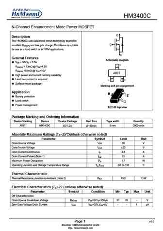
N-Channel Enhancement Mode Power MOSFET D Description The uses advanced trench technology to provide G excellent RDS(ON) and low gate charge .This device is suitable for use as a load switch or in PWM applications. S General Features Schematic diagram VDS = 30V,ID = 3.6A RDS(ON) ... See More ⇒
9.7. Size:679K cn hmsemi
hm3400dr.pdf
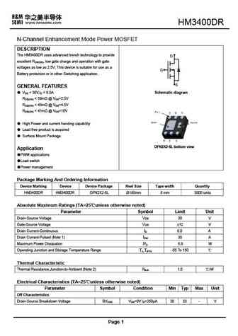
HM3400DR N-Channel Enhancement Mode Power MOSFET DESCRIPTION The HM3400DR uses advanced trench technology to provide D excellent RDS(ON), low gate charge and operation with gate voltages as low as 2.5V. This device is suitable for use as a G Battery protection or in other Switching application. S GENERAL FEATURES VDS = 30V,ID = 8 A Schematic diagram RDS(ON) ... See More ⇒
9.8. Size:459K cn hmsemi
hm3401b.pdf

HM3401B P-Channel Enhancement Mode Power MOSFET DESCRIPTION D The HM3401B uses advanced trench technology to provide excellent RDS(ON), low gate charge and operation with gate G voltages as low as 2.5V. This device is suitable for use as a load switch or in PWM applications. S Schematic diagram GENERAL FEATURES VDS = -30V,ID = -4.2A RDS(ON) ... See More ⇒
9.9. Size:446K cn hmsemi
hm3406b.pdf
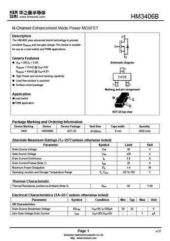
HM3406B N-Channel Enhancement Mode Power MOSFET Description D The HM3406 uses advanced trench technology to provide excellent RDS(ON) and low gate charge.This device is suitable G for use as a load switch and PWM applications. S Genera Features VDS = 30V,ID = 5.8A Schematic diagram RDS(ON) ... See More ⇒
9.10. Size:474K cn hmsemi
hm3400d.pdf
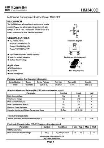
HM3400D N-Channel Enhancement Mode Power MOSFET DESCRIPTION The HM3400D uses advanced trench technology to provide D excellent RDS(ON), low gate charge and operation with gate voltages as low as 2.5V. This device is suitable for use as a G Battery protection or in other Switching application. S GENERAL FEATURES VDS = 30V,ID = 5.0A Schematic diagram RDS(ON) ... See More ⇒
9.11. Size:929K cn hmsemi
hm3401pr.pdf
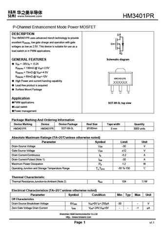
HM3401PR P-Channel Enhancement Mode Power MOSFET DESCRIPTION D The HM3401PR uses advanced trench technology to provide excellent RDS(ON), low gate charge and operation with gate G voltages as low as 2.5V. This device is suitable for use as a load switch or in PWM applications. S Schematic diagram GENERAL FEATURES VDS = -30V,ID = -5.2A RDS(ON) ... See More ⇒
9.12. Size:307K cn hmsemi
hm3400b.pdf

3400 N-Channel Enhancement Mode Power MOSFET DESCRIPTION The 3400 uses advanced trench technology to provide D excellent RDS(ON), low gate charge and operation with gate voltages as low as 2.5V. This device is suitable for use as a G Battery protection or in other Switching application. S GENERAL FEATURES VDS = 30V,ID = 5.8A Schematic diagram RDS(ON) ... See More ⇒
Detailed specifications: HM3400D, HM3400DR, HM3401, HM3401B, HM3401C, HM3401D, HM3401PR, HM3406B, 10N60, HM3407B, HM3413, HM3413B, HM3414, HM3414B, HM3415E, HM3416B, HM3421
Keywords - HM3407A MOSFET specs
HM3407A cross reference
HM3407A equivalent finder
HM3407A pdf lookup
HM3407A substitution
HM3407A replacement
Step-by-step guide to finding a MOSFET replacement. Cross-reference parts and ensure compatibility for your repair or project.