HM4884A Specs and Replacement
Type Designator: HM4884A
Type of Transistor: MOSFET
Type of Control Channel: N-Channel
Absolute Maximum Ratings
Pd ⓘ - Maximum Power Dissipation: 3 W
|Vds|ⓘ - Maximum Drain-Source Voltage: 40 V
|Vgs|ⓘ - Maximum Gate-Source Voltage: 20 V
|Id| ⓘ - Maximum Drain Current: 15 A
Tj ⓘ - Maximum Junction Temperature: 175 °C
Electrical Characteristics
tr ⓘ - Rise Time: 17.2 nS
Cossⓘ - Output Capacitance: 280 pF
RDSonⓘ - Maximum Drain-Source On-State Resistance: 0.013 Ohm
Package: SOP8
HM4884A substitution
- MOSFET ⓘ Cross-Reference Search
HM4884A datasheet
hm4884a.pdf
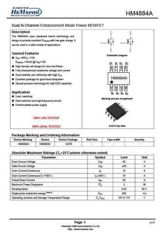
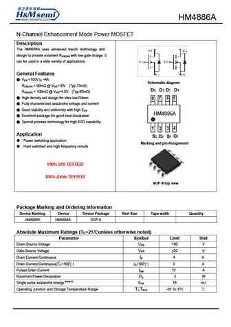
HM4884A Dual N-Channel Enhancement Mode Power MOSFET Description The HM4884A uses advanced trench technology and design to provide excellent RDS(ON) with low gate charge. It can be used in a wide variety of applications. General Features Schematic diagram VDS =40V,ID =15A RDS(ON) ... See More ⇒
hm4884.pdf
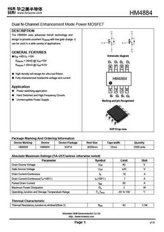
HM Dual N-Channel Enhancement Mode Power MOSFET DESCRIPTION The HM uses advanced trench technology and design to provide excellent RDS(ON) with low gate charge. It can be used in a wide variety of applications. GENERAL FEATURES Schematic diagram VDS =40V,ID =10A RDS(ON) ... See More ⇒
hm4885.pdf
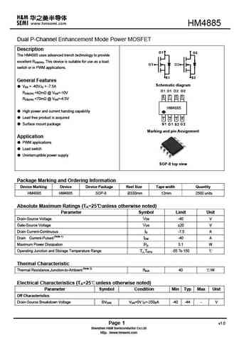
HM4885 Dual P-Channel Enhancement Mode Power MOSFET Description D1 D2 The HM4885 uses advanced trench technology to provide excellent RDS(ON), This device is suitable for use as a load G1 G2 switch or in PWM applications. S1 S2 General Features Schematic diagram VDS = -40V,ID = -7.5A RDS(ON) ... See More ⇒
hm4885a.pdf
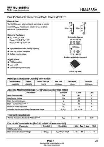
HM4885A Dual P-Channel Enhancement Mode Power MOSFET Description D1 D2 The HM4885A uses advanced trench technology to provide excellent RDS(ON), This device is suitable for use as a load G1 G2 switch or in PWM applications. S1 S2 General Features Schematic diagram VDS = -40V,ID = -13A RDS(ON) ... See More ⇒
Detailed specifications: HM4828A, HM4830, HM4840, HM4843, HM4853, HM4853A, HM4853B, HM4884, AO4407A, HM4885, HM4885A, HM4886A, HM4886E, HM4887, HM4892A, HM4892B, HM4922
Keywords - HM4884A MOSFET specs
HM4884A cross reference
HM4884A equivalent finder
HM4884A pdf lookup
HM4884A substitution
HM4884A replacement
Step-by-step guide to finding a MOSFET replacement. Cross-reference parts and ensure compatibility for your repair or project.
🌐 : EN ES РУ

LIST
Last Update
MOSFET: AUN084N10 | AUN065N10 | AUN063N10 | AUN062N08BG | AUN060N08AG | AUN053N10 | AUN050N08BGL | AUN045N085 | AUN042N055 | AUN036N10
Popular searches
a970 transistor | 2sb560 | tip31c transistor equivalent | 2sc1815 datasheet | mj15015 | 13003 transistor datasheet | 2n3416 | bdx53c