HM4892A Specs and Replacement
Type Designator: HM4892A
Type of Transistor: MOSFET
Type of Control Channel: N-Channel
Absolute Maximum Ratings
Pd ⓘ - Maximum Power Dissipation: 3 W
|Vds|ⓘ - Maximum Drain-Source Voltage: 100 V
|Vgs|ⓘ - Maximum Gate-Source Voltage: 20 V
|Id| ⓘ - Maximum Drain Current: 4.5 A
Tj ⓘ - Maximum Junction Temperature: 150 °C
Electrical Characteristics
tr ⓘ - Rise Time: 18 nS
Cossⓘ - Output Capacitance: 450 pF
RDSonⓘ - Maximum Drain-Source On-State Resistance: 0.037 Ohm
Package: SOP8
HM4892A substitution
- MOSFET ⓘ Cross-Reference Search
HM4892A datasheet
hm4892a.pdf
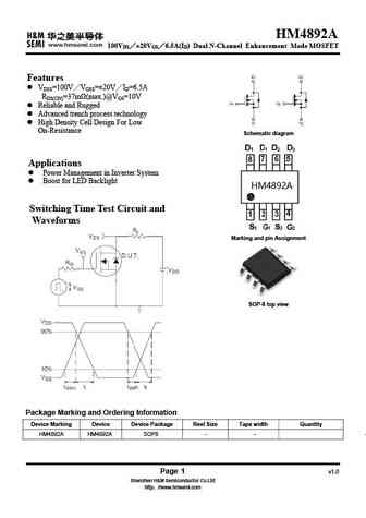
HM4892A 100VDS 20VGS 6.5A(ID) Dual N-Channel Enhancement Mode MOSFET Features VDSS=100V VGSS= 20V ID=6.5A RDS(ON)=37m (max.)@VGS=10V Reliable and Rugged Advanced trench process technology High Density Cell Design For Low On-Resistance Schematic diagram Applications Power Management in Inverter System Boost for LED Backlight H... See More ⇒
chm4892jgp.pdf
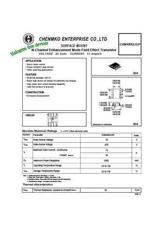
CHENMKO ENTERPRISE CO.,LTD CHM4892JGP SURFACE MOUNT N-Channel Enhancement Mode Field Effect Transistor VOLTAGE 30 Volts CURRENT 12 Ampere APPLICATION * Servo motor control. * Power MOSFET gate drivers. * Other switching applications. SO-8 FEATURE * Small flat package. (SO-8 ) ( ) * Super high dense cell design for extremely low RDS(ON). 4.06 0.160 ( ) 3.70 0.146 * High power ... See More ⇒
hm4892b.pdf
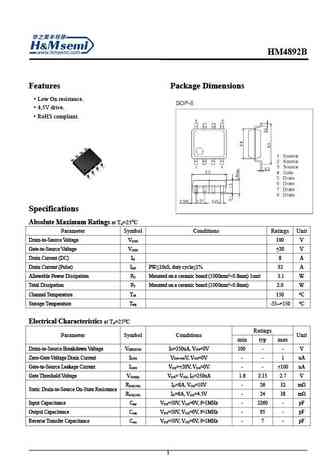
HM4892B Features Package Dimensions Low On resistance. 4.5V drive. RoHS compliant. Specifications Absolute Maximum Ratings at T =250C a Parameter Symbol Conditions Ratings Unit Drain-to-Source Voltage V 100 V DSS Gate-to-Source Voltage V +20 V GSS Drain Current (DC) I 8 A D Drain Current (Pulse) I PW 10uS, duty cycle 1% 32 A DP Allowable Power Dissipation P Mounted on... See More ⇒
Detailed specifications: HM4853B, HM4884, HM4884A, HM4885, HM4885A, HM4886A, HM4886E, HM4887, IRF3205, HM4892B, HM4922, HM4953, HM4953A, HM4953B, HM4953C, HM4953D, HM4963
Keywords - HM4892A MOSFET specs
HM4892A cross reference
HM4892A equivalent finder
HM4892A pdf lookup
HM4892A substitution
HM4892A replacement
Need a MOSFET replacement? Our guide shows you how to find a perfect substitute by comparing key parameters and specs
🌐 : EN ES РУ

LIST
Last Update
MOSFET: AUN084N10 | AUN065N10 | AUN063N10 | AUN062N08BG | AUN060N08AG | AUN053N10 | AUN050N08BGL | AUN045N085 | AUN042N055 | AUN036N10
Popular searches
2n3416 | bdx53c | k3563 | d882p | 2sb1560 | 2n1304 | 2sa979 | 2sc4793