HM8810S Datasheet. Specs and Replacement
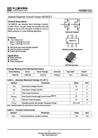
Type Designator: HM8810S 📄📄
Type of Transistor: MOSFET
Type of Control Channel: N-Channel
Absolute Maximum Ratings
Pd ⓘ - Maximum Power Dissipation: 1.5 W
|Vds|ⓘ - Maximum Drain-Source Voltage: 20 V
|Vgs|ⓘ - Maximum Gate-Source Voltage: 12 V
|Id| ⓘ - Maximum Drain Current: 5 A
Tj ⓘ - Maximum Junction Temperature: 150 °C
Electrical Characteristics
tr ⓘ - Rise Time: 12 nS
Cossⓘ - Output Capacitance: 315 pF
RDSonⓘ - Maximum Drain-Source On-State Resistance: 0.022 Ohm
Package: SOT23-6
📄📄 Copy
HM8810S substitution
- MOSFET ⓘ Cross-Reference Search
HM8810S datasheet
hm8810s.pdf
HM8810S Dual N-Channel Trench Power MOSFET General Description The HM8810S uses advanced trench technology to provide excellent R , low gate charge and operation with gate DS(ON) voltages as low as 2.5V. This device is suitable for use as a Battery protection or in other Switching applications. Schematic Diagram Features VDS = 20V,ID =5A HM8810S R ... See More ⇒
hm8810e.pdf
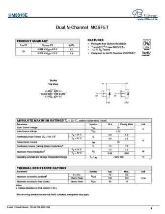
HM8810E www.VBsemi.tw Dual N-Channel MOSFET FEATURES PRODUCT SUMMARY Halogen-free Option Available VDS (V) RDS(on) ( )ID (A) Pb-free TrenchFET Power MOSFETs 0.024 at VGS = 4.5 V Available 6.0 100 % Rg Tested 20 RoHS* 0.028 at VGS = 2.5 V Compliant to RoHS Directive 2002/95/EC 5.0 COMPLIANT TSOP6 D D Top View S1 1 6 G1 D1/D2 2 5 D1/D2 G1 G2 S2 G2 3 4... See More ⇒
hm8810a.pdf
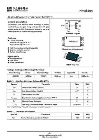
HM Dual N-Channel Trench Power MOSFET General Description The HM uses advanced trench technology to provide excellent R , low gate charge and operation with gate DS(ON) voltages as low as 2.5V. This device is suitable for use as a Battery protection or in other Switching applications. Schematic Diagram Features VDS = 20V,ID =7A HM R ... See More ⇒
hm8810e.pdf
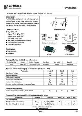
HM8810E Dual N-Channel Enhancement Mode Power MOSFET Description The HM8810E uses advanced trench technology to provide excellent RDS(ON), low gate charge and operation with gate voltages as low as 2.5V. This device is suitable for use as a load switch or in PWM applications .It is ESD protested. Schematic diagram General Features VDS = 20V,ID =7A RDS(ON) ... See More ⇒
Detailed specifications: HM85N02K, HM85N80, HM85N90, HM85N95D, HM85P02, HM85P02D, HM85P02K, HM8810A, IRFB3206, HM8N20, HM8N20A, HM8N20I, HM8N20K, HM8N20KA, HM8N25K, HM8P02MR, HM90N04D
Keywords - HM8810S MOSFET specs
HM8810S cross reference
HM8810S equivalent finder
HM8810S pdf lookup
HM8810S substitution
HM8810S replacement
Need a MOSFET replacement? Our guide shows you how to find a perfect substitute by comparing key parameters and specs
MOSFET Parameters. How They Affect Each Other
🌐 : EN ES РУ
LIST
Last Update
MOSFET: CS95118 | CS85105A | CS75N45 | CS72N12 | CS55N50 | CS48N75A | CS40N27 | MSQ60P04D | MSQ40P07D | MSQ30P40D
Popular searches
ksc2073 | nte102a | tip31cg | s9015 transistor | irf540z | ss8550 transistor | irfp240 mosfet | tip141


