HMS110N15 Datasheet. Specs and Replacement
Type Designator: HMS110N15 📄📄
Type of Transistor: MOSFET
Type of Control Channel: N-Channel
Absolute Maximum Ratings
Pd ⓘ - Maximum Power Dissipation: 300 W
|Vds|ⓘ - Maximum Drain-Source Voltage: 135 V
|Vgs|ⓘ - Maximum Gate-Source Voltage: 20 V
|Id| ⓘ - Maximum Drain Current: 110 A
Tj ⓘ - Maximum Junction Temperature: 175 °C
Electrical Characteristics
tr ⓘ - Rise Time: 52 nS
Cossⓘ - Output Capacitance: 2046 pF
RDSonⓘ - Maximum Drain-Source On-State Resistance: 0.007 Ohm
Package: TO220
HMS110N15 substitution
- MOSFET ⓘ Cross-Reference Search
HMS110N15 datasheet
hms110n15.pdf
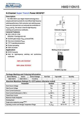
HMS110N15 N-Channel Super Trench Power MOSFET Description The HMS110N15 uses Super Trench technology that is uniquely optimized to provide the most efficient high frequency switching performance. Both conduction and switching power losses are minimized due to an extremely low combination of RDS(ON) and Qg. This device is ideal for high-frequency switching and synchronous rectific... See More ⇒
hms11n60d hms11n60 hms11n60f.pdf
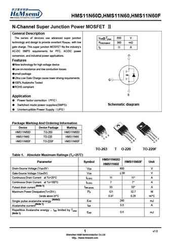
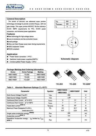
HMS11N60D,HMS11N60,HMS11N60F N-Channel Super Junction Power MOSFET General Description The series of devices use advanced super junction 650 V VDS@Tjmax technology and design to provide excellent RDS(ON) with low RDS(ON)MAX 360 m gate charge. This super junction MOSFET fits the industry s ID 11 A AC-DC SMPS requirements for PFC, AC/DC power conversion, and industrial p... See More ⇒
hms11n60k hms11n60i.pdf

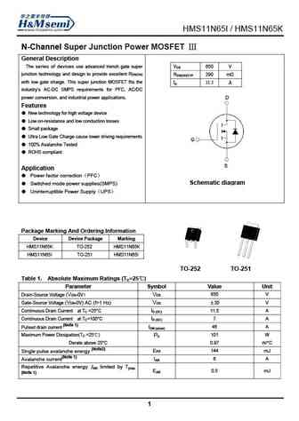
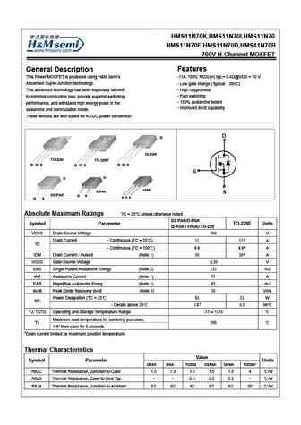
HMS11N60K/HMS11N60I HMS11N60K/HMS11N60I 600V N-Channel MOSFET General Description Features This Power MOSFET is produced using H&M Semi s - 11A, 600V, RDS(on) typ. = 0.34 @VGS = 10 V Advanced Super-Junction technology. - Low gate charge ( typical 33nC) This advanced technology has been especially tailored - High ruggedness to minimize conduction loss, provide superior switching - Fast... See More ⇒
hms11n65k hms11n65i.pdf
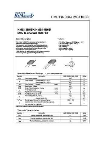
HMS11N65K/HMS11N65I HMS11N65K/HMS11N65I 650V N-Channel MOSFET General Description Features This Power MOSFET is produced using H&M Semi s - 11A, 650V, RDS(on) typ. = 0.38 @VGS = 10 V Advanced Super-Junction technology. - Low gate charge ( typical 33nC) This advanced technology has been especially tailored - High ruggedness to minimize conduction loss, provide superior switching - Fast... See More ⇒
Detailed specifications: HM9436, HM9926, HM9926B, HM9N90F, HMS100N85D, HMS105N10D, HMS10N60I, HMS10N60K, IRF640N, HMS11N60, HMS11N60D, HMS11N60F, HMS11N60I, HMS11N60K, HMS11N65, HMS11N65D, HMS11N65F
Keywords - HMS110N15 MOSFET specs
HMS110N15 cross reference
HMS110N15 equivalent finder
HMS110N15 pdf lookup
HMS110N15 substitution
HMS110N15 replacement
Can't find your MOSFET? Learn how to find a substitute transistor by analyzing voltage, current and package compatibility
