ME1302AT3 Specs and Replacement
Type Designator: ME1302AT3
Type of Transistor: MOSFET
Type of Control Channel: N-Channel
Absolute Maximum Ratings
Pd ⓘ - Maximum Power Dissipation: 0.42 W
|Vds|ⓘ - Maximum Drain-Source Voltage: 30 V
|Vgs|ⓘ - Maximum Gate-Source Voltage: 12 V
|Id| ⓘ - Maximum Drain Current: 1.4 A
Tj ⓘ - Maximum Junction Temperature: 150 °C
Electrical Characteristics
tr ⓘ - Rise Time: 41.9 nS
Cossⓘ - Output Capacitance: 21 pF
RDSonⓘ - Maximum Drain-Source On-State Resistance: 0.132 Ohm
Package: SOT323
ME1302AT3 substitution
- MOSFET ⓘ Cross-Reference Search
ME1302AT3 datasheet
me1302at3 me1302at3-g.pdf
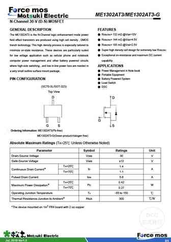
ME1302AT3/ME1302AT3-G N-Channel 30-V (D-S) MOSFET GENERAL DESCRIPTION FEATURES The ME1302AT3 is the N-Channel logic enhancement mode power RDS(ON)= 132 m @VGS=10V field effect transistors are produced using high cell density , DMOS RDS(ON)= 144 m @VGS=4.5V trench technology. This high density process is especially tailored to RDS(ON)= 185 m @VGS=2.5V minimize on... See More ⇒
me1303at3 me1303at3-g.pdf
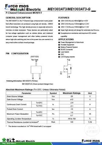
ME1303AT3/ME1303AT3-G P-Channel Enhancement MOSFET GENERAL DESCRIPTION FEATURES The ME1303AT3 is the P-Channel logic enhancement mode power -20V/-3.4A,RDS(ON)=95m @VGS=-4.5V field effect transistors are produced using high cell density , DMOS -20V/-2.4A,RDS(ON)=120m @VGS=-2.5V trench technology. This high density process is especially tailored to -20V/-1.7A,RDS(ON)=180... See More ⇒
Detailed specifications: JCS740BC, JCS740CC, JCS740FC, FTP11N08A, JY09M, ME100N03T, ME100N03T-G, ME120N04T, IRLZ44N, ME1302AT3-G, ME1303AT3, ME1303AT3-G, ME13N10A, ME13N10A-G, ME15N25, ME15N25F, ME15N25F-G
Keywords - ME1302AT3 MOSFET specs
ME1302AT3 cross reference
ME1302AT3 equivalent finder
ME1302AT3 pdf lookup
ME1302AT3 substitution
ME1302AT3 replacement
Learn how to find the right MOSFET substitute. A guide to cross-reference, check specs and replace MOSFETs in your circuits.
History: ME120N04T
🌐 : EN ES РУ

LIST
Last Update
MOSFET: AKF30N5P0SX | AKF30N10S | AKF20P45D | CM4407 | CM3407 | CM3400 | SVF11N65F | SVF11N65T | FKBB3105 | EHBA036R1
Popular searches
a970 | d2390 transistor | 2n5087 equivalent | tip147 datasheet | 2n4124 | mj15022 | toshiba c5198 | irf520n datasheet