ME2312-G Specs and Replacement
Type Designator: ME2312-G
Type of Transistor: MOSFET
Type of Control Channel: N-Channel
Absolute Maximum Ratings
Pd ⓘ - Maximum Power Dissipation: 1.3 W
|Vds|ⓘ - Maximum Drain-Source Voltage: 20 V
|Vgs|ⓘ - Maximum Gate-Source Voltage: 8 V
|Id| ⓘ - Maximum Drain Current: 5.1 A
Tj ⓘ - Maximum Junction Temperature: 150 °C
Electrical Characteristics
tr ⓘ - Rise Time: 17 nS
Cossⓘ - Output Capacitance: 85.7 pF
RDSonⓘ - Maximum Drain-Source On-State Resistance: 0.033 Ohm
Package: SOT23
ME2312-G substitution
- MOSFET ⓘ Cross-Reference Search
ME2312-G datasheet
me2312 me2312-g.pdf
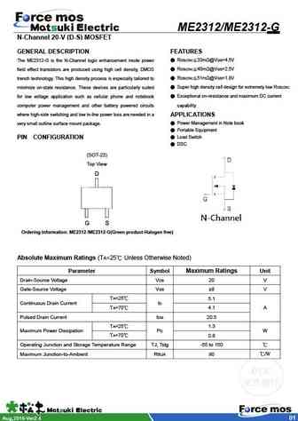
ME2312/ME2312-G N-Channel 20-V (D-S) MOSFET GENERAL DESCRIPTION FEATURES The ME2312-G is the N-Channel logic enhancement mode power RDS(ON) 33m @VGS=4.5V field effect transistors are produced using high cell density, DMOS RDS(ON) 40m @VGS=2.5V trench technology. This high density process is especially tailored to RDS(ON) 51m @VGS=1.8V minimize on-state resist... See More ⇒
me2313 me2313-g.pdf
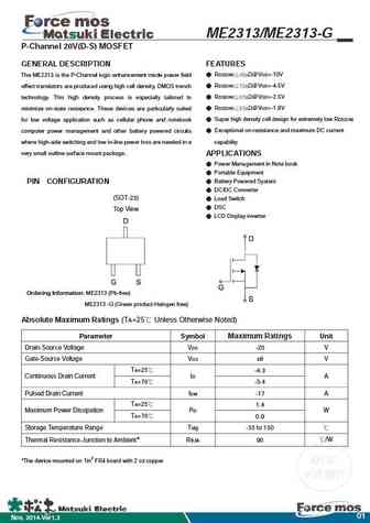
ME2313/ME2313-G P-Channel 20V(D-S) MOSFET BSS84 GENERAL DESCRIPTION FEATURES The ME2313 is the P-Channel logic enhancement mode power field RDS(ON) 48m @VGS=-10V effect transistors are produced using high cell density, DMOS trench RDS(ON) 52m @VGS=-4.5V technology. This high density process is especially tailored to RDS(ON) 65m @VGS=-2.5V minimize on-state r... See More ⇒
me2310.pdf
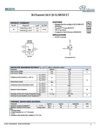
ME2310 www.VBsemi.tw N-Channel 30-V (D-S) MOSFET FEATURES PRODUCT SUMMARY Halogen-free According to IEC 61249-2-21 VDS (V) RDS(on) ( ) ID (A)a Qg (Typ.) Definition 0.030 at VGS = 10 V TrenchFET Power MOSFET 6.5 30 4.5 nC 100 % Rg Tested 0.033 at VGS = 4.5 V 6.0 Compliant to RoHS Directive 2002/95/EC APPLICATIONS DC/DC Converter D TO-236 (SOT-23) G 1... See More ⇒
Detailed specifications: ME2306N, ME2306N-G, ME2306S, ME2306S-G, ME2308D, ME2308D-G, ME2308DN-G, ME2312, IRF1407, ME2313, ME2313-G, ME2320D2-G, ME2320DS, ME2320DS-G, ME2324D, ME2324D-G, ME2325S
Keywords - ME2312-G MOSFET specs
ME2312-G cross reference
ME2312-G equivalent finder
ME2312-G pdf lookup
ME2312-G substitution
ME2312-G replacement
Need a MOSFET replacement? Our guide shows you how to find a perfect substitute by comparing key parameters and specs
History: IPP100N10S3-05 | UTT30P06G-TQ2-R
🌐 : EN ES РУ

LIST
Last Update
MOSFET: CM4407 | CM3407 | CM3400 | SVF11N65F | SVF11N65T | FKBB3105 | EHBA036R1 | CRTT067N10N | AP6NA3R2MT | AP65SA145DDT8
Popular searches
2n3416 | bdx53c | k3563 | d882p | 2sb1560 | 2n1304 | 2sa979 | 2sc4793