HFI50N06A Datasheet. Specs and Replacement
Type Designator: HFI50N06A 📄📄
Type of Transistor: MOSFET
Type of Control Channel: N-Channel
Absolute Maximum Ratings
Pd ⓘ - Maximum Power Dissipation: 120 W
|Vds|ⓘ - Maximum Drain-Source Voltage: 60 V
|Vgs|ⓘ - Maximum Gate-Source Voltage: 25 V
|Id| ⓘ - Maximum Drain Current: 50 A
Tj ⓘ - Maximum Junction Temperature: 175 °C
Electrical Characteristics
|VGSth|ⓘ - Maximum Gate-Threshold Voltage: 4 V
Qg ⓘ - Total Gate Charge: 27 nC
tr ⓘ - Rise Time: 105 nS
Cossⓘ - Output Capacitance: 445 pF
RDSonⓘ - Maximum Drain-Source On-State Resistance: 0.022 Ohm
Package: TO262
HFI50N06A substitution
- MOSFET ⓘ Cross-Reference Search
HFI50N06A datasheet
hfi50n06a hfw50n06a.pdf
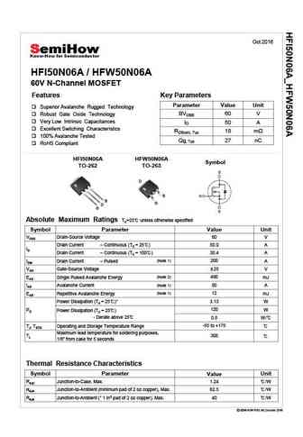
Oct 2016 HFI50N06A / HFW50N06A 60V N-Channel MOSFET Features Key Parameters Parameter Value Unit Superior Avalanche Rugged Technology BVDSS 60 V Robust Gate Oxide Technology Very Low Intrinsic Capacitances ID 50 A Excellent Switching Characteristics RDS(on), Typ 18 100% Avalanche Tested Qg, Typ 27 nC RoHS Compliant HFI50N06A HFW50N06A Symbol TO-262 TO-263 D S ... See More ⇒
hfi50n06 hfw50n06.pdf
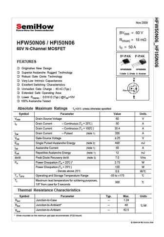
Nov 2009 BVDSS = 60 V RDS(on) = 18 m HFW50N06 / HFI50N06 ID = 50 A 60V N-Channel MOSFET D2-PAK I2-PAK FEATURES Originative New Design HFW50N06 HFI50N06 Superior Avalanche Rugged Technology 1.Gate 2. Drain 3. Source Robust Gate Oxide Technology Very Low Intrinsic Capacitances Excellent Switching Characteristics Unrivalled Gate Charge 40 nC (Typ.) Extended Safe Operati... See More ⇒
Detailed specifications: HFB1N60F, HFC2N60U, HFD1N60F, HFD1N60SA, HFD2N60F, HFD5N60F, HFD5N65SA, HFH9N90A, IRF520, HFI5N50S, HFI5N60S, HFP2N60F, HFP4N60F, HFP50N06A, HFP5N60F, HFP730F, HFP830F
Keywords - HFI50N06A MOSFET specs
HFI50N06A cross reference
HFI50N06A equivalent finder
HFI50N06A pdf lookup
HFI50N06A substitution
HFI50N06A replacement
Can't find your MOSFET? Learn how to find a substitute transistor by analyzing voltage, current and package compatibility
🌐 : EN ES РУ

LIST
Last Update
MOSFET: ASDM30DN30E | ASDM3050KQ | ASDM2305 | ASDM2301 | ASDM2300ZA | ASDM20P13S | ASDM20N90Q | ASDM20N60 | ASDM7002EZA | ASDM68N80KQ
Popular searches
bf495 transistor equivalent | 2sc1313 | 2sb560 replacement | 2sd330 replacement | a1273 transistor | 2sc1384 equivalent | 2sd786 | a940 transistor