HFU5N40 Datasheet. Specs and Replacement
Type Designator: HFU5N40 📄📄
Type of Transistor: MOSFET
Type of Control Channel: N-Channel
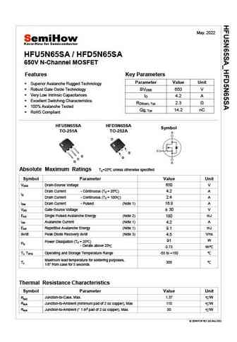
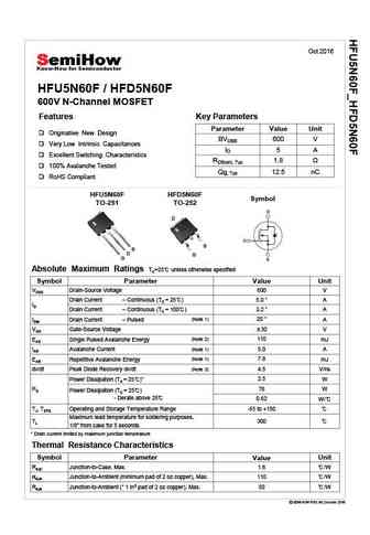
Absolute Maximum Ratings
Pd ⓘ - Maximum Power Dissipation: 45 W
|Vds|ⓘ - Maximum Drain-Source Voltage: 400 V
|Vgs|ⓘ - Maximum Gate-Source Voltage: 30 V
|Id| ⓘ - Maximum Drain Current: 3.4 A
Tj ⓘ - Maximum Junction Temperature: 150 °C
Electrical Characteristics
tr ⓘ - Rise Time: 70 nS
Cossⓘ - Output Capacitance: 70 pF
RDSonⓘ - Maximum Drain-Source On-State Resistance: 1.6 Ohm
Package: IPAK
HFU5N40 substitution
- MOSFET ⓘ Cross-Reference Search
HFU5N40 datasheet
hfd5n40 hfu5n40.pdf
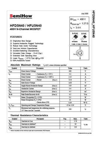
July 2005 BVDSS = 400 V RDS(on) typ HFD5N40 / HFU5N40 ID = 3.4 A 400V N-Channel MOSFET D-PAK I-PAK 2 FEATURES 1 1 3 2 3 Originative New Design HFD5N40 HFU5N40 Superior Avalanche Rugged Technology 1.Gate 2. Drain 3. Source Robust Gate Oxide Technology Very Low Intrinsic Capacitances Excellent Switching Characteristics Unrivalled Gate Charge 13 nC (Typ... See More ⇒
hfd5n60s hfu5n60s.pdf
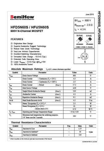
June 2015 BVDSS = 600 V RDS(on) typ HFD5N60S / HFU5N60S ID = 4.3 A 600V N-Channel MOSFET D-PAK I-PAK 2 FEATURES 1 1 3 2 3 Originative New Design HFD5N60S HFU5N60S Superior Avalanche Rugged Technology 1.Gate 2. Drain 3. Source Robust Gate Oxide Technology Very Low Intrinsic Capacitances Excellent Switching Characteristics Unrivalled Gate Charge 10.5 nC... See More ⇒
hfd5n50s hfu5n50s.pdf
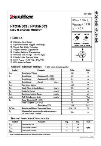
OCT 2009 BVDSS = 500 V RDS(on) typ HFD5N50S / HFU5N50S ID = 4.0 A 500V N-Channel MOSFET D-PAK I-PAK 2 FEATURES 1 1 3 2 3 Originative New Design HFD5N50S HFU5N50S Superior Avalanche Rugged Technology 1.Gate 2. Drain 3. Source Robust Gate Oxide Technology Very Low Intrinsic Capacitances Excellent Switching Characteristics Unrivalled Gate Charge 15.5 nC ... See More ⇒
hfd5n60u hfu5n60u.pdf
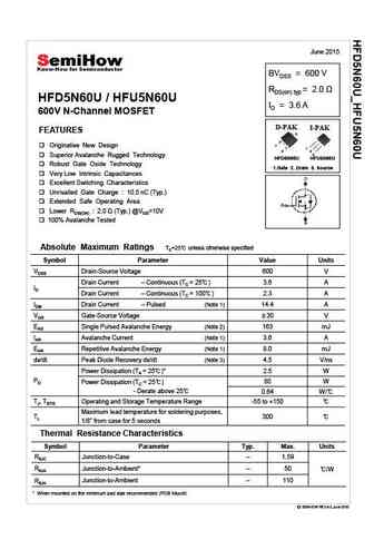
June 2015 BVDSS = 600 V RDS(on) typ = 2.0 HFD5N60U / HFU5N60U ID = 3.6 A 600V N-Channel MOSFET D-PAK I-PAK FEATURES 2 1 Originative New Design 1 3 2 3 Superior Avalanche Rugged Technology HFD5N60U HFU5N60U Robust Gate Oxide Technology 1.Gate 2. Drain 3. Source Very Low Intrinsic Capacitances Excellent Switching Characteristics Unrivalled Gate Charge 10.5 nC... See More ⇒

Detailed specifications: HFT1N60F, HFU1N60F, HFU1N60S, HFU1N60SA, HFU2N60F, HFU2N60S, HFU2N60U, HFU4N50, IRFZ44, HFU5N50S, HFU5N50U, HFU5N60F, HFU5N60S, HFU5N60U, HFU5N65SA, HFW50N06A, HFW840
Keywords - HFU5N40 MOSFET specs
HFU5N40 cross reference
HFU5N40 equivalent finder
HFU5N40 pdf lookup
HFU5N40 substitution
HFU5N40 replacement
Need a MOSFET replacement? Our guide shows you how to find a perfect substitute by comparing key parameters and specs
🌐 : EN ES РУ

LIST
Last Update
MOSFET: ASDM30DN30E | ASDM3050KQ | ASDM2305 | ASDM2301 | ASDM2300ZA | ASDM20P13S | ASDM20N90Q | ASDM20N60 | ASDM7002EZA | ASDM68N80KQ
Popular searches
7506 mosfet datasheet | 2sb1186a | a1695 datasheet | 3415 transistor | 072ne6pt | 2sd388 | 2sc1400 | 2sd331