FDN5618P Specs and Replacement
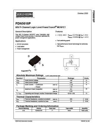
Type Designator: FDN5618P
Type of Transistor: MOSFET
Type of Control Channel: P-Channel
Absolute Maximum Ratings
Pd ⓘ - Maximum Power Dissipation: 0.5 W
|Vds|ⓘ - Maximum Drain-Source Voltage: 60 V
|Vgs|ⓘ - Maximum Gate-Source Voltage: 20 V
|Id| ⓘ - Maximum Drain Current: 1.25 A
Tj ⓘ - Maximum Junction Temperature: 150 °C
Electrical Characteristics
tr ⓘ - Rise Time: 8 nS
Cossⓘ - Output Capacitance: 52 pF
RDSonⓘ - Maximum Drain-Source On-State Resistance: 0.17 Ohm
Package: SSOT3
FDN5618P substitution
- MOSFET ⓘ Cross-Reference Search
FDN5618P datasheet
fdn5618p.pdf
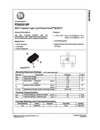
FDN5618P 60V P-Channel Logic Level PowerTrench MOSFET General Description Features This 60V P-Channel MOSFET uses ON 1.25 A, 60 V. RDS(ON) = 0.170 @ VGS = 10 V Semiconductor s high voltage PowerTrench process. It RDS(ON) = 0.230 @ VGS = 4.5 V has been optimized for power management applications. Fast switching speed Applications Hi... See More ⇒
fdn5632n f085.pdf
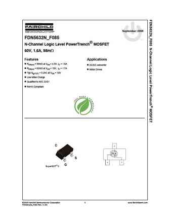
September 2008 FDN5632N_F085 tm N-Channel Logic Level PowerTrench MOSFET 60V, 1.6A, 98m Features Applications RDS(on) = 98m at VGS = 4.5V, ID = 1.6A DC/DC converter RDS(on) = 82m at VGS = 10V, ID = 1.7A Motor Drives Typ Qg(TOT) = 9.2nC at VGS = 10V Low Miller Charge Qualified to AEC Q101 RoHS Compliant 2008 Fairchild Semiconductor Corporation 1 www.fairchild... See More ⇒
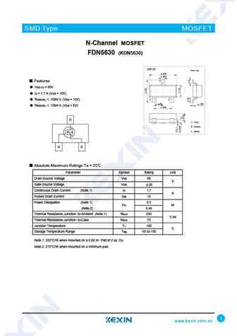
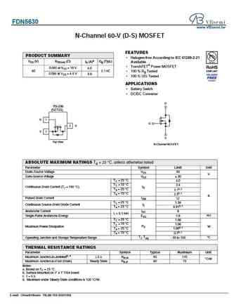
fdn5630.pdf
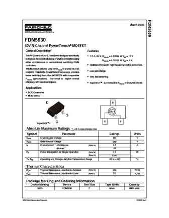
March 2000 FDN5630 60V N-Channel PowerTrench MOSFET General Description Features This N-Channel MOSFET has been designed specifically 1.7 A, 60 V. RDS(ON) = 0.100 @ VGS = 10 V to improve the overall efficiency of DC/DC converters using RDS(ON) = 0.120 @ VGS = 6 V. either synchronous or conventional switching PWM Optimized for use in high frequenc... See More ⇒
Detailed specifications: FDN342P, FDN352AP, FDN359BN, STM4884A, FDN361BN, STM4884, FDN372S, STM4880, IRF2807, FDN5630, FDN8601, STM4840, FDN86246, FDP025N06, FDP030N06, FDP032N08, FDP036N10A
Keywords - FDN5618P MOSFET specs
FDN5618P cross reference
FDN5618P equivalent finder
FDN5618P pdf lookup
FDN5618P substitution
FDN5618P replacement
Step-by-step guide to finding a MOSFET replacement. Cross-reference parts and ensure compatibility for your repair or project.
History: FDN8601 | SI1305EDL | STK801 | RUH120N35L | ZXMP6A17DN8
🌐 : EN ES РУ
LIST
Last Update
MOSFET: AUB034N10 | AUB033N08BG | AUB026N085 | AUA062N08BG | AUA060N08AG | AUA056N08BGL | AUA039N10 | ASW80R290E | ASW65R120EFD | ASW65R110E
Popular searches
irfp4568 | mj15004 | ksc2073 | nte102a | tip31cg | s9015 transistor | irf540z | ss8550 transistor
