FDN5630 Datasheet. Specs and Replacement
Type Designator: FDN5630 📄📄
Type of Transistor: MOSFET
Type of Control Channel: N-Channel
Absolute Maximum Ratings
Pd ⓘ - Maximum Power Dissipation: 0.5 W
|Vds|ⓘ - Maximum Drain-Source Voltage: 60 V
|Vgs|ⓘ - Maximum Gate-Source Voltage: 20 V
|Id| ⓘ - Maximum Drain Current: 1.7 A
Tj ⓘ - Maximum Junction Temperature: 150 °C
Electrical Characteristics
tr ⓘ - Rise Time: 6 nS
Cossⓘ - Output Capacitance: 102 pF
RDSonⓘ - Maximum Drain-Source On-State Resistance: 0.1 Ohm
Package: SSOT3
📄📄 Copy
FDN5630 substitution
- MOSFET ⓘ Cross-Reference Search
FDN5630 datasheet
fdn5630.pdf
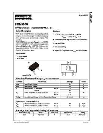
March 2000 FDN5630 60V N-Channel PowerTrench MOSFET General Description Features This N-Channel MOSFET has been designed specifically 1.7 A, 60 V. RDS(ON) = 0.100 @ VGS = 10 V to improve the overall efficiency of DC/DC converters using RDS(ON) = 0.120 @ VGS = 6 V. either synchronous or conventional switching PWM Optimized for use in high frequenc... See More ⇒
fdn5630.pdf
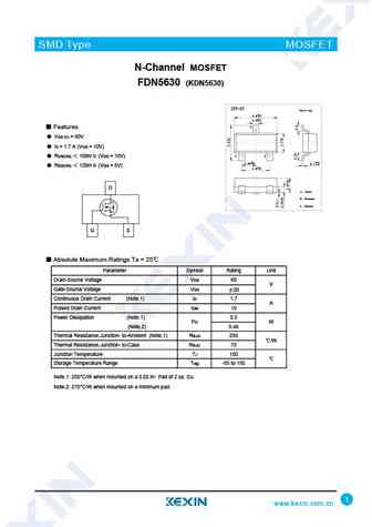
SMD Type MOSFET N-Channel MOSFET FDN5630 (KDN5630) SOT-23 Unit mm +0.1 2.9 -0.1 +0.1 0.4 -0.1 3 Features VDS (V) = 60V ID = 1.7 A (VGS = 10V) 1 2 RDS(ON) 100m (VGS = 10V) +0.1 +0.05 0.95-0.1 0.1-0.01 RDS(ON) 120m (VGS = 6V) +0.1 1.9-0.1 D 1. Gate 2. Source 3. Drain G S Absolute Maximum Ratings Ta = 25 Parameter Symbol Rating... See More ⇒
fdn5630.pdf
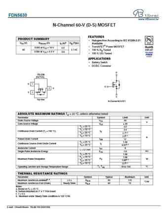
FDN5630 www.VBsemi.tw N-Channel 60-V (D-S) MOSFET FEATURES PRODUCT SUMMARY Halogen-free According to IEC 61249-2-21 VDS (V) RDS(on) ( ) ID (A)a Qg (Typ.) Available TrenchFET Power MOSFET 0.085 at VGS = 10 V 4.0 60 2.1 nC 100 % Rg Tested 0.096 at VGS = 4.5 V 3.8 100 % UIS Tested APPLICATIONS Battery Switch DC/DC Converter D TO-236 (SOT23) G 1 ... See More ⇒
fdn5630-3.pdf

SMD Type MOSFET N-Channel MOSFET FDN5630 (KDN5630) SOT-23-3 Unit mm +0.2 2.9-0.1 +0.1 0.4 -0.1 3 Features VDS (V) = 60V ID = 1.7 A (VGS = 10V) 1 2 RDS(ON) 100m (VGS = 10V) +0.02 +0.1 0.15 -0.02 0.95 -0.1 +0.1 1.9-0.2 RDS(ON) 120m (VGS = 6V) 1. Gate D 2. Source 3. Drain G S Absolute Maximum Ratings Ta = 25 Parameter Symbol Ra... See More ⇒

Detailed specifications: FDN352AP, FDN359BN, STM4884A, FDN361BN, STM4884, FDN372S, STM4880, FDN5618P, STF13NM60N, FDN8601, STM4840, FDN86246, FDP025N06, FDP030N06, FDP032N08, FDP036N10A, STM4639
Keywords - FDN5630 MOSFET specs
FDN5630 cross reference
FDN5630 equivalent finder
FDN5630 pdf lookup
FDN5630 substitution
FDN5630 replacement
Learn how to find the right MOSFET substitute. A guide to cross-reference, check specs and replace MOSFETs in your circuits.
