ASDM30N65E-R Specs and Replacement
Type Designator: ASDM30N65E-R
Type of Transistor: MOSFET
Type of Control Channel: N-Channel
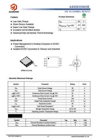
Absolute Maximum Ratings
Pd ⓘ - Maximum Power Dissipation: 25 W
|Vds|ⓘ - Maximum Drain-Source Voltage: 30 V
|Vgs|ⓘ - Maximum Gate-Source Voltage: 20 V
|Id| ⓘ - Maximum Drain Current: 32 A
Tj ⓘ - Maximum Junction Temperature: 150 °C
Electrical Characteristics
tr ⓘ - Rise Time: 18.8 nS
Cossⓘ - Output Capacitance: 436 pF
RDSonⓘ - Maximum Drain-Source On-State Resistance: 0.0052 Ohm
Package: DFN3.3X3.3-8L
ASDM30N65E-R substitution
- MOSFET ⓘ Cross-Reference Search
ASDM30N65E-R datasheet
asdm30n65e-r.pdf

ASDM30N65E 30V N-CHANNEL MOSFET Product Summary Feature l Low Gate Charge VDS 30 V l Green Device Available 4.5 m RDS(on),typ VGS=10V l Super Low Gate Charge A 65 ID l Excellent CdV/dt effect decline l Advanced high cell density Trench technology Applications l Power Management in Desktop Computer or DC/DC Converters. l Isolated DC/DC Converters in Telecom and Industrial. ... See More ⇒
asdm30n65e.pdf
ASDM30N65E 30V N-CHANNEL MOSFET Product Summary Feature l Low Gate Charge VDS 30 V l Green Device Available 4.5 m RDS(on),typ VGS=10V l Super Low Gate Charge A 65 ID l Excellent CdV/dt effect decline l Advanced high cell density Trench technology Applications l Power Management in Desktop Computer or DC/DC Converters. l Isolated DC/DC Converters in Telecom and Industrial. ... See More ⇒
asdm30n55e-r.pdf
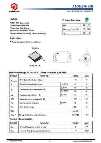
ASDM30N55E 30V N-CHANNEL MOSFET Feature Product Summary 100% EAS Guaranteed VDS 30 V Green Device Available Super Low Gate Charge RDS(on),typ VGS=10V 4.8 m Excellent CdV/dt effect decline A 55 ID Advanced high cell density Trench technology Application Power Management in Inverter System top view DFN3.3*3.3-8 Maximum ratings, at T A=25 C, unless othe... See More ⇒
asdm30n90kq.pdf
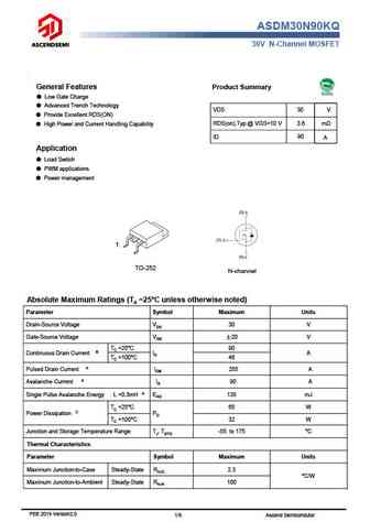
ASDM30N90KQ 30V N-Channel MOSFET General Features Product Summary Low Gate Charge Advanced Trench Technology VDS 30 V Provide Excellent RDS(ON) RDS(on),Typ.@ VGS=10 V 3.6 m High Power and Current Handling Capability 90 ID A Application Load Swtich PWM applications Power management 1 TO-252 N-channel Absolute Maximum Ratings (TA =25 C unless o... See More ⇒

Detailed specifications: AP80N04G, AP80N04Q, AP90N03Q, AP90P03G, AP90P03Q, APG077N01G, APG095N01G, ASDM30N55E-R, IRLZ44N, ASDM30P11TD-R, ASDM30P30CTD-R, ASDM40N52E-R, AUIRFN8405TR, CJAC100SN08U, CJAC110SN10A, CJAC80SN10, DMN3009LFVW-7
Keywords - ASDM30N65E-R MOSFET specs
ASDM30N65E-R cross reference
ASDM30N65E-R equivalent finder
ASDM30N65E-R pdf lookup
ASDM30N65E-R substitution
ASDM30N65E-R replacement
Learn how to find the right MOSFET substitute. A guide to cross-reference, check specs and replace MOSFETs in your circuits.
🌐 : EN ES РУ

LIST
Last Update
MOSFET: ASU70R600E | ASU65R850E | ASU65R550E | ASU65R350E | ASR65R120EFD | ASR65R046EFD | ASQ65R046EFD | ASM65R280E | ASM60R330E | ASE70R950E
Popular searches
d331 transistor | irfbc40 | mp16b transistor | 2sa934 | 2sd118 | 2n3403 | 2sa750 | tip117