HYG019N04NR1C2 Specs and Replacement
Type Designator: HYG019N04NR1C2
Type of Transistor: MOSFET
Type of Control Channel: N-Channel
Absolute Maximum Ratings
Pd ⓘ - Maximum Power Dissipation: 79 W
|Vds|ⓘ - Maximum Drain-Source Voltage: 40 V
|Vgs|ⓘ - Maximum Gate-Source Voltage: 20 V
|Id| ⓘ - Maximum Drain Current: 127 A
Tj ⓘ - Maximum Junction Temperature: 175 °C
Electrical Characteristics
tr ⓘ - Rise Time: 84 nS
Cossⓘ - Output Capacitance: 596 pF
RDSonⓘ - Maximum Drain-Source On-State Resistance: 0.0025 Ohm
Package: PDFN5X6-8L
HYG019N04NR1C2 substitution
- MOSFET ⓘ Cross-Reference Search
HYG019N04NR1C2 datasheet
hyg019n04nr1c2.pdf
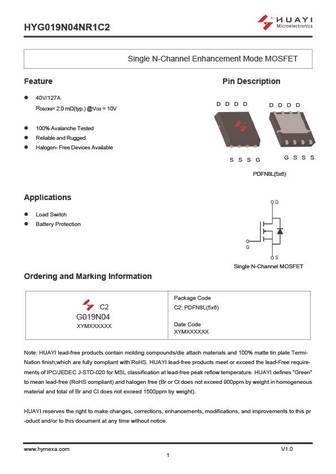
HYG019N04NR1C2 Single N-Channel Enhancement Mode MOSFET Feature Pin Description 40V/127A D D D D D D D D RDS(ON)= 2.0 m (typ.) @VGS = 10V 100% Avalanche Tested Reliable and Rugged Halogen- Free Devices Available G S S S S S S G PDFN8L(5x6) Applications Load Switch Battery Protection Single N-Channel MOSFET Ordering and Marking Information Package Code ... See More ⇒
hyg017n04ls1c2.pdf

HYG017N04LS1C2 Single N-Channel Enhancement Mode MOSFET Feature Description Pin Description 40V/135A D D D D D D D D RDS(ON)= 1.7m (typ.) @VGS = 10V RDS(ON)= 2.3m (typ.) @VGS = 4.5V 100% Avalanche Tested Reliable and Rugged Halogen- Free Devices Available G S S S S S S G Pin1 PDFN5*6-8L Applications Switching Application Power Manageme... See More ⇒
hyg015n04ls1c2.pdf
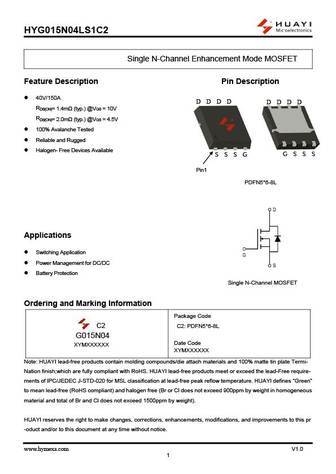
HYG015N04LS1C2 Single N-Channel Enhancement Mode MOSFET Feature Description Pin Description 40V/150A D D D D D D D D RDS(ON)= 1.4m (typ.) @VGS = 10V RDS(ON)= 2.0m (typ.) @VGS = 4.5V 100% Avalanche Tested Reliable and Rugged Halogen- Free Devices Available G S S S S S S G Pin1 PDFN5*6-8L Applications Switching Application Power Manageme... See More ⇒
hyg013n03ls1c2.pdf

HYG013N03LS1C2 Single N-Channel Enhancement Mode MOSFET Feature Description Pin Description 30V/150A D D D D D D D D RDS(ON)= 1.3m (typ.) @VGS = 10V RDS(ON)= 2.0m (typ.) @VGS = 4.5V 100% Avalanche Tested Reliable and Rugged Halogen- Free Devices Available G S S S S S S G Pin1 PDFN5*6-8L Applications Switching Application Power Manageme... See More ⇒

Detailed specifications: HSBB6254, HY1906C2, HYG007N03LS1C2, HYG009N04LS1C2, HYG011N04LS1C2, HYG013N03LS1C2, HYG015N04LS1C2, HYG017N04LS1C2, 2N60, HYG023N03LR1C2, HYG025N04NA1C2, HYG045N03LA1C1, HYG055N08NS1C2, HYG072N10LS1C2, HYG110P04LQ2C2, IPLK60R1K0PFD7, IPLK60R1K5PFD7
Keywords - HYG019N04NR1C2 MOSFET specs
HYG019N04NR1C2 cross reference
HYG019N04NR1C2 equivalent finder
HYG019N04NR1C2 pdf lookup
HYG019N04NR1C2 substitution
HYG019N04NR1C2 replacement
Can't find your MOSFET? Learn how to find a substitute transistor by analyzing voltage, current and package compatibility
🌐 : EN ES РУ

LIST
Last Update
MOSFET: FTF30P35D | FTF25N35DHVT | FTF15N35D | FTE15C35G | FTP02P15G | FTE02P15G | AKF30N5P0SX | AKF30N10S | AKF20P45D | CM4407
Popular searches
2sc2389 | b331 transistor | 2sa720 | 2sc1345 | 2sd555 | a950 transistor | k2611 | c1740 transistor