WMN12N100C2 Specs and Replacement
Type Designator: WMN12N100C2
Type of Transistor: MOSFET
Type of Control Channel: N-Channel
Absolute Maximum Ratings
Pd ⓘ - Maximum Power Dissipation: 150 W
|Vds|ⓘ - Maximum Drain-Source Voltage: 1000 V
|Vgs|ⓘ - Maximum Gate-Source Voltage: 30 V
|Id| ⓘ - Maximum Drain Current: 6.8 A
Tj ⓘ - Maximum Junction Temperature: 150 °C
Electrical Characteristics
tr ⓘ - Rise Time: 32 nS
Cossⓘ - Output Capacitance: 49 pF
RDSonⓘ - Maximum Drain-Source On-State Resistance: 0.8 Ohm
Package: TO262
WMN12N100C2 substitution
- MOSFET ⓘ Cross-Reference Search
WMN12N100C2 datasheet
wml12n100c2 wmm12n100c2 wmn12n100c2 wmj12n100c2 wmk12n100c2.pdf
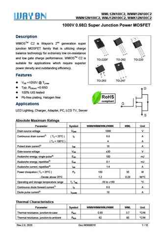
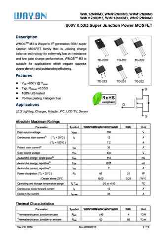
WML12N100C2, WMM C2 W M12N100C WMN12N WMJ12N10 K12N100C N100C2, W 00C2, WMK C2 1000V 0.68 S unction Power M T Super Ju MOSFET Descrip ption WMOSTM C2 is Wa 2nd generation super ayon s n junction MOSFET fa that is utilizing charge M amily S balance te or extremely esistance echnology fo y low on-re S D D G G G S D G and low ga charge performanc WMOSTM C... See More ⇒
wml12n105c2 wmm12n105c2 wmn12n105c2 wmj12n105c2 wmk12n105c2.pdf
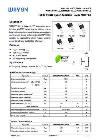
WML12N105C2, WMM12N105C2 WMN12N105C2, WMJ12N105C2, WMK12N105C2 1050V 0.68 Super Junction Power MOSFET Description WMOSTM C2 is Wayon s 2nd generation super junction MOSFET family that is utilizing charge S balance technology for extremely low on-resistance S D D G G S D G and low gate charge performance. WMOSTM C2 is TO-220F TO-262 TO-220 suitable for applic... See More ⇒
swmn12n65da.pdf
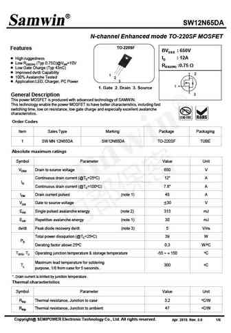
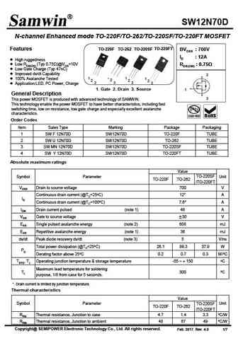
SW12N65DA N-channel Enhanced mode TO-220SF MOSFET TO-220SF Features BVDSS 650V ID 12A High ruggedness Low RDS(ON) (Typ 0.75 )@VGS=10V RDS(ON) 0.75 Low Gate Charge (Typ 43nC) Improved dv/dt Capability 2 1 100% Avalanche Tested 2 3 Application LED, Charger, PC Power 1 1. Gate 2. Drain 3. Source 3 General Description Th... See More ⇒
swmn12n65d swy12n65d.pdf
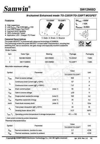
SW12N65D N-channel Enhanced mode TO-220SF/TO-220FT MOSFET TO-220SF TO-220FT BVDSS 650V Features ID 12A High ruggedness RDS(ON) 0.66 Low RDS(ON) (Typ 0.66 )@VGS=10V Low Gate Charge (Typ 41nC) 2 Improved dv/dt Capability 1 1 100% Avalanche Tested 2 1 2 3 3 Application LED , Charger, PC Power 1. Gate 2. Drain 3. Source... See More ⇒

Detailed specifications: WMN11N80M3, WMM11N80M3, WMO11N80M3, WMP11N80M3, WMK11N80M3, WML125N12LG2, WML12N100C2, WMM12N100C2, SKD502T, WMJ12N100C2, WMK12N100C2, WML12N105C2, WMM12N105C2, WMN12N105C2, WMJ12N105C2, WMK12N105C2, WML12N65D1
Keywords - WMN12N100C2 MOSFET specs
WMN12N100C2 cross reference
WMN12N100C2 equivalent finder
WMN12N100C2 pdf lookup
WMN12N100C2 substitution
WMN12N100C2 replacement
Need a MOSFET replacement? Our guide shows you how to find a perfect substitute by comparing key parameters and specs
History: WML13N70EM | BUK7624-55 | IRLZ44SPBF | IRFB61N15D
🌐 : EN ES РУ

LIST
Last Update
MOSFET: ASU70R600E | ASU65R850E | ASU65R550E | ASU65R350E | ASR65R120EFD | ASR65R046EFD | ASQ65R046EFD | ASM65R280E | ASM60R330E | ASE70R950E
Popular searches
c3998 | c4468 datasheet | 2sc2603 | jcs50n20wt | 2sa1360 | p60nf06 datasheet | 2sc4468 | ru6888r