FDS3672 Datasheet. Specs and Replacement
Type Designator: FDS3672 📄📄
Type of Transistor: MOSFET
Type of Control Channel: N-Channel
Absolute Maximum Ratings
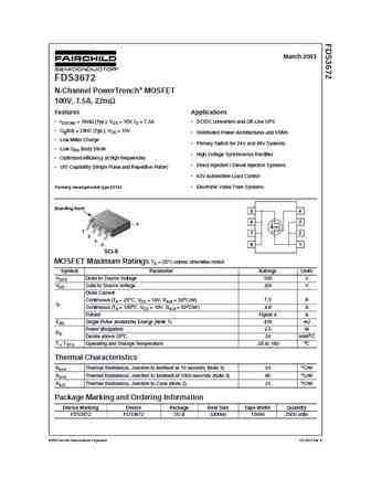
Pd ⓘ - Maximum Power Dissipation: 2.5 W
|Vds|ⓘ - Maximum Drain-Source Voltage: 100 V
|Vgs|ⓘ - Maximum Gate-Source Voltage: 20 V
|Id| ⓘ - Maximum Drain Current: 7.5 A
Tj ⓘ - Maximum Junction Temperature: 150 °C
Electrical Characteristics
tr ⓘ - Rise Time: 20 nS
Cossⓘ - Output Capacitance: 285 pF
RDSonⓘ - Maximum Drain-Source On-State Resistance: 0.023 Ohm
Package: SO-8
📄📄 Copy
FDS3672 substitution
- MOSFET ⓘ Cross-Reference Search
FDS3672 datasheet
fds3672.pdf
March 2003 FDS3672 N-Channel PowerTrench MOSFET 100V, 7.5A, 22m Features Applications rDS(ON) = 19m (Typ.), VGS = 10V, ID = 7.5A DC/DC converters and Off-Line UPS Qg(tot) = 28nC (Typ.), VGS = 10V Distributed Power Architectures and VRMs Low Miller Charge Primary Switch for 24V and 48V Systems Low QRR Body Diode High Voltage Synchronous Rectifie... See More ⇒
fds3672.pdf
Is Now Part of To learn more about ON Semiconductor, please visit our website at www.onsemi.com Please note As part of the Fairchild Semiconductor integration, some of the Fairchild orderable part numbers will need to change in order to meet ON Semiconductor s system requirements. Since the ON Semiconductor product management systems do not have the ability to manage part nomenclatur... See More ⇒
fds3672.pdf
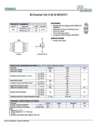
FDS3672 www.VBsemi.tw N-Channel 100 V (D-S) MOSFET FEATURES PRODUCT SUMMARY Halogen-free According to IEC 61249-2-21 VDS (V) RDS(on) ( )ID (A)a Qg (Typ.) Definition 0.040 at VGS = 10 V 6.4 Extremely Low Qgd for Switching Losses 100 23 nC 0.047 at VGS = 8 V 5.5 100 % Rg Tested 100 % Avalanche Tested Compliant to RoHS Directive 2002/95/EC D APPLICATIONS SO-8... See More ⇒
fds3670.pdf
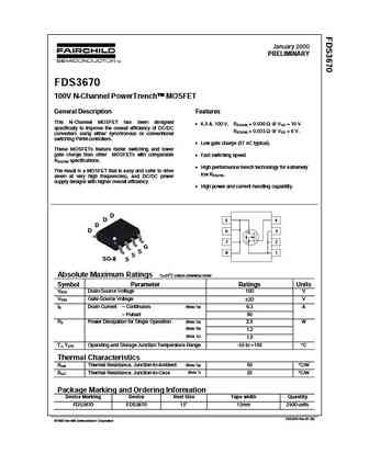
January 2000 PRELIMINARY FDS3670 100V N-Channel PowerTrench MOSFET General Description Features This N-Channel MOSFET has been designed 6.3 A, 100 V. RDS(ON) = 0.030 @ VGS = 10 V specifically to improve the overall efficiency of DC/DC RDS(ON) = 0.033 @ VGS = 6 V. converters using either synchronous or conventional switching PWM controllers. Low gate charge (57 nC typ... See More ⇒
Detailed specifications: FDS2672, STF2455, FDS2672F085, STF2454A, FDS2734, FDS3512, FDS3572, FDS3590, AO4407A, STF2454, FDS3692, STF06N20, FDS3890, FDS3992, STE339S, FDS4141, FDS4141F085
Keywords - FDS3672 MOSFET specs
FDS3672 cross reference
FDS3672 equivalent finder
FDS3672 pdf lookup
FDS3672 substitution
FDS3672 replacement
Need a MOSFET replacement? Our guide shows you how to find a perfect substitute by comparing key parameters and specs
MOSFET Parameters. How They Affect Each Other
History: HGB049N10S | NTR4503NT1
🌐 : EN ES РУ
LIST
Last Update
MOSFET: CS95118 | CS85105A | CS75N45 | CS72N12 | CS55N50 | CS48N75A | CS40N27 | MSQ60P04D | MSQ40P07D | MSQ30P40D
Popular searches
a1023 datasheet | 2sc1080 | 2sb618 | 2sc1328 | 2sc1845 transistor | a933 transistor datasheet | a1633 transistor | 2sa844
