FDS4685 Specs and Replacement
Type Designator: FDS4685
Type of Transistor: MOSFET
Type of Control Channel: P-Channel
Absolute Maximum Ratings
Pd ⓘ - Maximum Power Dissipation: 2.5 W
|Vds|ⓘ - Maximum Drain-Source Voltage: 40 V
|Vgs|ⓘ - Maximum Gate-Source Voltage: 20 V
|Id| ⓘ - Maximum Drain Current: 8.2 A
Tj ⓘ - Maximum Junction Temperature: 150 °C
Electrical Characteristics
tr ⓘ - Rise Time: 11 nS
Cossⓘ - Output Capacitance: 256 pF
RDSonⓘ - Maximum Drain-Source On-State Resistance: 0.027 Ohm
Package: SO-8
FDS4685 substitution
- MOSFET ⓘ Cross-Reference Search
FDS4685 datasheet
fds4685.pdf
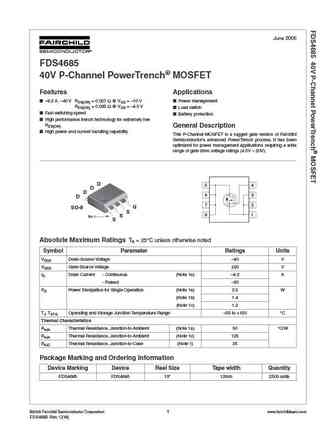
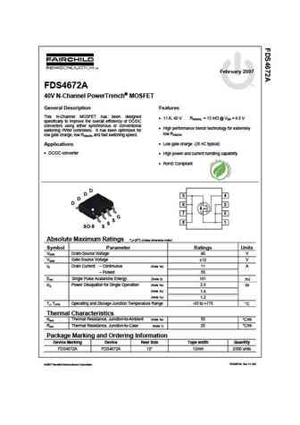
June 2005 FDS4685 40V P-Channel PowerTrench MOSFET Features Applications 8.2 A, 40 V RDS(ON) = 0.027 @ VGS = 10 V Power management RDS(ON) = 0.035 @ VGS = 4.5 V Load switch Fast switching speed Battery protection High performance trench technology for extremely low RDS(ON) General Description High power and current handling capabi... See More ⇒
fds4685.pdf
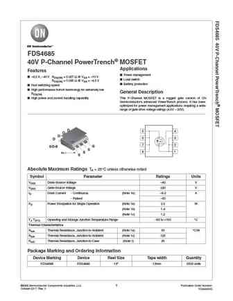
FDS4685 40V P-Channel PowerTrench MOSFET Applications Features Power management 8.2 A, 40 V RDS(ON) = 0.027 @ VGS = 10 V Load switch RDS(ON) = 0.035 @ VGS = 4.5 V Battery protection Fast switching speed High performance trench technology for extremely low General Description RDS(ON) High power and current handling capability This P-... See More ⇒
fds4685-nl.pdf
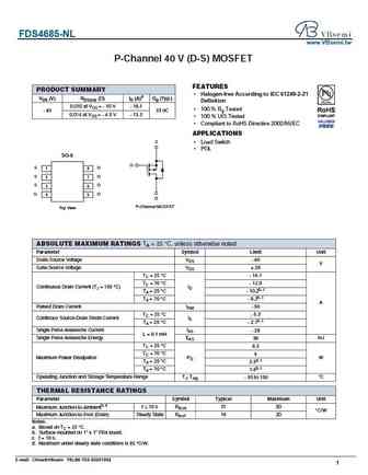
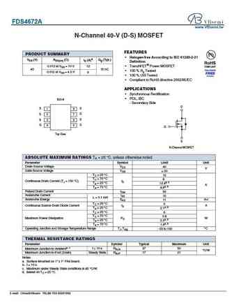
FDS4685-NL www.VBsemi.tw P-Channel 40 V (D-S) MOSFET FEATURES PRODUCT SUMMARY Halogen-free According to IEC 61249-2-21 VDS (V) RDS(on) ( )ID (A)a Qg (Typ.) Definition 0.010 at VGS = - 10 V - 16.1 100 % Rg Tested - 40 33 nC 0.014 at VGS = - 4.5 V - 13.3 100 % UIS Tested Compliant to RoHS Directive 2002/95/EC APPLICATIONS S Load Switch POL SO-8 G SD ... See More ⇒
fds4675.pdf
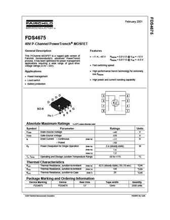
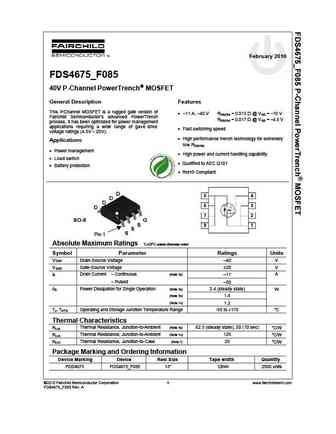
February 2001 FDS4675 40V P-Channel PowerTrench MOSFET General Description Features This P MOSFET is a rugged gate version of -Channel 11 A, 40 V R = 0.013 @ V = 10 V DS(ON) GS Fairchild Semiconductor s advanced PowerTrench R = 0.017 @ V = 4.5 V DS(ON) GS process. It has been optimized for power management applications requiring a wide range of g... See More ⇒
Detailed specifications: STB458D, STB440S, FDS4559, STB438S, FDS4559F085, STB438A, FDS4672A, FDS4675F085, AO3400A, FDS4897AC, STB434S, FDS4897C, STB432S, FDS4935A, FDS4935BZ, FDS5351, FDS5670
Keywords - FDS4685 MOSFET specs
FDS4685 cross reference
FDS4685 equivalent finder
FDS4685 pdf lookup
FDS4685 substitution
FDS4685 replacement
Can't find your MOSFET? Learn how to find a substitute transistor by analyzing voltage, current and package compatibility
🌐 : EN ES РУ
LIST
Last Update
MOSFET: AUB062N08BG | AUB060N08AG | AUB056N10 | AUB056N08BGL | AUB050N085 | AUB050N055 | AUB045N12 | AUB045N10BT | AUB039N10 | AUB034N10
Popular searches
bt152 datasheet | 2sa1302 datasheet | mpsa13 transistor equivalent | кт817г характеристики | 2sc1972 | 2n5088 transistor equivalent | 2n5884 | bc640
