NCEP023N10T Datasheet. Specs and Replacement
Type Designator: NCEP023N10T
Type of Transistor: MOSFET
Type of Control Channel: N-Channel
Absolute Maximum Ratings
Pd ⓘ - Maximum Power Dissipation: 365 W
|Vds|ⓘ - Maximum Drain-Source Voltage: 100 V
|Vgs|ⓘ - Maximum Gate-Source Voltage: 20 V
|Id| ⓘ - Maximum Drain Current: 280 A
Tj ⓘ - Maximum Junction Temperature: 175 °C
Electrical Characteristics
tr ⓘ - Rise Time: 29 nS
Cossⓘ - Output Capacitance: 1500 pF
RDSonⓘ - Maximum Drain-Source On-State Resistance: 0.0024 Ohm
Package: TO-247
NCEP023N10T substitution
- MOSFET ⓘ Cross-Reference Search
NCEP023N10T datasheet
ncep023n10t.pdf
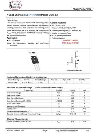
NCEP023N10T NCE N-Channel Super Trench II Power MOSFET Description The series of devices uses Super Trench II technology that is General Features uniquely optimized to provide the most efficient high frequency V =100V,I =280A DS D switching performance. Both conduction and switching power R =1.85m , typical@ V =10V DS(ON) GS losses are minimized due to an extremely low combinati... See More ⇒
ncep023n10d.pdf
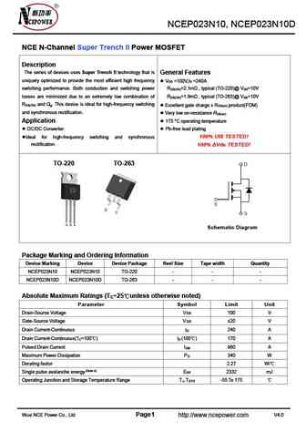
NCEP023N10, NCEP023N10D NCE N-Channel Super Trench II Power MOSFET Description The series of devices uses Super Trench II technology that is General Features uniquely optimized to provide the most efficient high frequency V =100V,I =240A DS D switching performance. Both conduction and switching power R =2.1m , typical (TO-220)@ V =10V DS(ON) GS losses are minimized due to an ext... See More ⇒
ncep023n10 ncep023n10d.pdf

NCEP023N10, NCEP023N10D NCE N-Channel Super Trench II Power MOSFET Description The series of devices uses Super Trench II technology that is General Features uniquely optimized to provide the most efficient high frequency VDS =100V,ID =240A switching performance. Both conduction and switching power RDS(ON)=2.0m , typical (TO-220)@ VGS=10V losses are minimized due to an ext... See More ⇒
ncep023n10ll.pdf
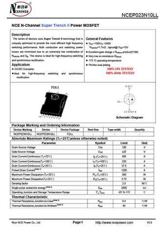
NCEP023N10LL NCE N-Channel Super Trench II Power MOSFET Description The series of devices uses Super Trench II technology that is General Features uniquely optimized to provide the most efficient high frequency VDS =100V,ID =300A switching performance. Both conduction and switching power RDS(ON)=1.7m , typical@ VGS=10V losses are minimized due to an extremely low combinat... See More ⇒

Detailed specifications: NCEP0212F, NCEP0218G, NCEP0218K, NCEP0220F, NCEP0225F, NCEP0225G, NCEP0225K, NCEP0230D, 60N06, NCEP023N85M, NCEP023N85T, NCEP023NH30GU, NCEP02503S, NCEP02505S, NCEP02515F, NCEP02525G, NCEP02525K
Keywords - NCEP023N10T MOSFET specs
NCEP023N10T cross reference
NCEP023N10T equivalent finder
NCEP023N10T pdf lookup
NCEP023N10T substitution
NCEP023N10T replacement
Learn how to find the right MOSFET substitute. A guide to cross-reference, check specs and replace MOSFETs in your circuits.
