NCEP026N10D Datasheet. Specs and Replacement
Type Designator: NCEP026N10D
Type of Transistor: MOSFET
Type of Control Channel: N-Channel
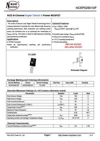
Absolute Maximum Ratings
Pd ⓘ - Maximum Power Dissipation: 300 W
|Vds|ⓘ - Maximum Drain-Source Voltage: 100 V
|Vgs|ⓘ - Maximum Gate-Source Voltage: 20 V
|Id| ⓘ - Maximum Drain Current: 200 A
Tj ⓘ - Maximum Junction Temperature: 175 °C
Electrical Characteristics
tr ⓘ - Rise Time: 27 nS
Cossⓘ - Output Capacitance: 1100 pF
RDSonⓘ - Maximum Drain-Source On-State Resistance: 0.0026 Ohm
Package: TO-263
NCEP026N10D substitution
- MOSFET ⓘ Cross-Reference Search
NCEP026N10D datasheet
ncep026n10d.pdf
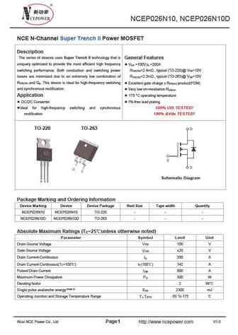
NCEP026N10, NCEP026N10D NCE N-Channel Super Trench II Power MOSFET Description The series of devices uses Super Trench II technology that is General Features uniquely optimized to provide the most efficient high frequency V =100V,I =200A DS D switching performance. Both conduction and switching power R =2.4m , typical (TO-220)@ V =10V DS(ON) GS losses are minimized due to an ext... See More ⇒
ncep026n10 ncep026n10d.pdf

NCEP026N10, NCEP026N10D NCE N-Channel Super Trench II Power MOSFET Description The series of devices uses Super Trench II technology that is General Features uniquely optimized to provide the most efficient high frequency V =100V,I =200A DS D switching performance. Both conduction and switching power R =2.4m , typical (TO-220)@ V =10V DS(ON) GS losses are minimized due to an ext... See More ⇒
ncep026n10m.pdf
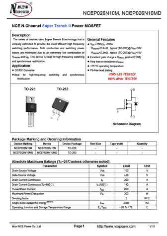
NCEP026N10M, NCEP026N10MD NCE N-Channel Super Trench II Power MOSFET Description The series of devices uses Super Trench II technology that is General Features uniquely optimized to provide the most efficient high frequency VDS =100V,ID =200A switching performance. Both conduction and switching power RDS(ON)=2.4m , typical (TO-220)@ VGS=10V losses are minimized due to an ... See More ⇒
ncep026n10ll.pdf
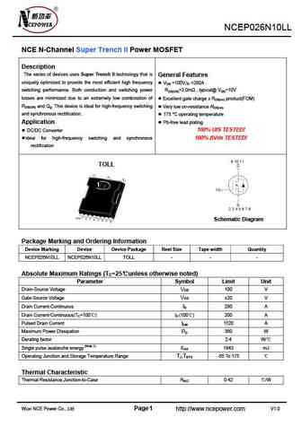
NCEP026N10LL NCE N-Channel Super Trench II Power MOSFET Description The series of devices uses Super Trench II technology that is General Features uniquely optimized to provide the most efficient high frequency VDS =100V,ID =280A switching performance. Both conduction and switching power RDS(ON)=2.0m , typical@ VGS=10V losses are minimized due to an extremely low combinat... See More ⇒
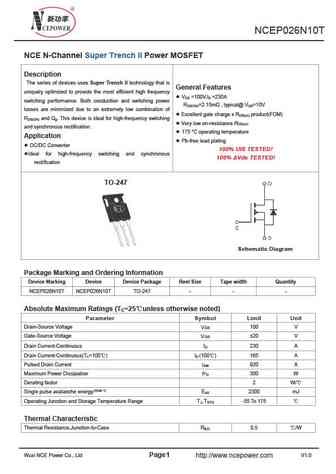

Detailed specifications: NCEP025N60, NCEP025N60AG, NCEP025N60D, NCEP025N60G, NCEP025N85LL, NCEP0260, NCEP0260D, NCEP026N10, IRFB4115, NCEP026N10F, NCEP026N10LL, NCEP026N10M, NCEP026N10T, NCEP026N85, NCEP026N85D, NCEP028N12LL, NCEP028N60AGU
Keywords - NCEP026N10D MOSFET specs
NCEP026N10D cross reference
NCEP026N10D equivalent finder
NCEP026N10D pdf lookup
NCEP026N10D substitution
NCEP026N10D replacement
Need a MOSFET replacement? Our guide shows you how to find a perfect substitute by comparing key parameters and specs
🌐 : EN ES РУ

LIST
Last Update
MOSFET: RM50P30DF | CRTT095N12N | CRSS028N10N | CRST030N10N | CRJQ80N65F | ASDM20N20KQ | ASDM20N100Q | ASDM12N65F | ASDM100R750PKQ | ASDM100R160NKQ
Popular searches
a1016 transistor | a1693 transistor | a933 datasheet | c535 transistor | irf3205 reemplazo | mpsu06 | кт630 | 2g381 transistor