NCEP040NH150LL Datasheet. Specs and Replacement
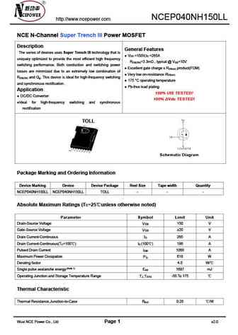
Type Designator: NCEP040NH150LL
Type of Transistor: MOSFET
Type of Control Channel: N-Channel
Absolute Maximum Ratings
Pd ⓘ
- Maximum Power Dissipation: 618 W
|Vds|ⓘ - Maximum Drain-Source Voltage: 150 V
|Vgs|ⓘ - Maximum Gate-Source Voltage: 20 V
|Id| ⓘ - Maximum Drain Current: 265 A
Tj ⓘ - Maximum Junction Temperature: 175 °C
Electrical Characteristics
tr ⓘ - Rise Time: 40 nS
Cossⓘ -
Output Capacitance: 2050 pF
RDSonⓘ - Maximum Drain-Source On-State Resistance: 0.004 Ohm
Package: TOLL
NCEP040NH150LL substitution
- MOSFET ⓘ Cross-Reference Search
NCEP040NH150LL datasheet
..1. Size:756K ncepower
ncep040nh150ll.pdf 

NCEP040NH150LL http //www.ncepower.com NCE N-Channel Super Trench III Power MOSFET Description General Features The series of devices uses Super Trench III technology that is V =150V,I =265A DS D uniquely optimized to provide the most efficient high frequency R =3.3m , typical @ V =10V DS(ON) GS switching performance. Both conduction and switching power Excellent gate char... See More ⇒
6.1. Size:400K ncepower
ncep040n12d.pdf 

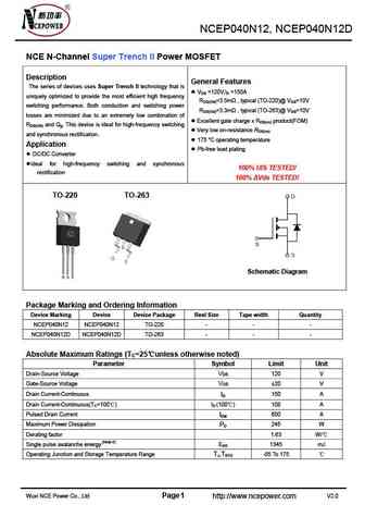
NCEP040N12, NCEP040N12D NCE N-Channel Super Trench II Power MOSFET Description General Features The series of devices uses Super Trench II technology that is VDS =120V,ID =150A uniquely optimized to provide the most efficient high frequency RDS(ON)=3.5m , typical (TO-220)@ VGS=10V switching performance. Both conduction and switching power RDS(ON)=3.3m , typical (TO-2... See More ⇒
6.2. Size:363K ncepower
ncep040n10.pdf 

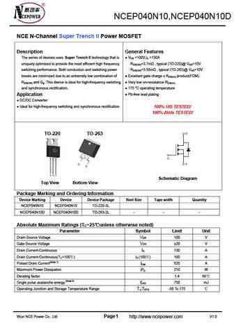
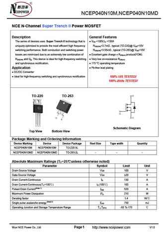
NCEP040N10,NCEP040N10D NCE N-Channel Super Trench II Power MOSFET Description General Features The series of devices uses Super Trench II technology that is VDS =100V,ID =130A uniquely optimized to provide the most efficient high frequency RDS(ON)=3.7m , typical (TO-220)@ VGS=10V switching performance. Both conduction and switching power RDS(ON)=3.55m , typical (TO-263)@ VGS=... See More ⇒
6.3. Size:363K ncepower
ncep040n10d.pdf 

NCEP040N10,NCEP040N10D NCE N-Channel Super Trench II Power MOSFET Description General Features The series of devices uses Super Trench II technology that is VDS =100V,ID =130A uniquely optimized to provide the most efficient high frequency RDS(ON)=3.7m , typical (TO-220)@ VGS=10V switching performance. Both conduction and switching power RDS(ON)=3.55m , typical (TO-263)@ VGS=... See More ⇒
6.4. Size:699K ncepower
ncep040n85.pdf 

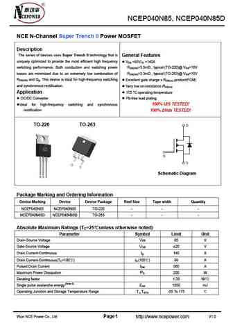
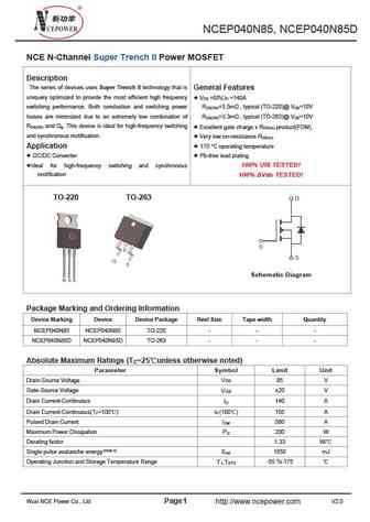
NCEP040N85, NCEP040N85D NCE N-Channel Super Trench II Power MOSFET Description The series of devices uses Super Trench II technology that is General Features uniquely optimized to provide the most efficient high frequency V =85V,I =140A DS D switching performance. Both conduction and switching power R =3.5m , typical (TO-220)@ V =10V DS(ON) GS losses are minimized due to an extr... See More ⇒
6.5. Size:1002K ncepower
ncep040n85m.pdf 

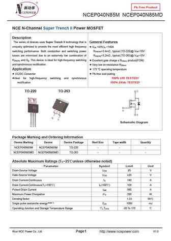
Pb Free Product NCEP040N85M NCEP040N85MD NCE N-Channel Super Trench II Power MOSFET Description The series of devices uses Super Trench II technology that is General Features uniquely optimized to provide the most efficient high frequency V =85V,I =140A DS D switching performance. Both conduction and switching power R =3.4m , typical (TO-220)@ V =10V DS(ON) GS losses are minimi... See More ⇒
6.6. Size:1002K ncepower
ncep040n85md.pdf 

Pb Free Product NCEP040N85M NCEP040N85MD NCE N-Channel Super Trench II Power MOSFET Description The series of devices uses Super Trench II technology that is General Features uniquely optimized to provide the most efficient high frequency V =85V,I =140A DS D switching performance. Both conduction and switching power R =3.4m , typical (TO-220)@ V =10V DS(ON) GS losses are minimi... See More ⇒
6.7. Size:1123K ncepower
ncep040n85g.pdf 

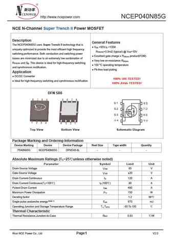
http //www.ncepower.com NCEP040N85G NCE N-Channel Super Trench II Power MOSFET Description General Features The NCEP040N85G uses Super Trench II technology that is V =85V,I =120A DS D uniquely optimized to provide the most efficient high frequency R =3.5m (typical) @ V =10V DS(ON) GS switching performance. Both conduction and switching power Excellent gate charge x R produc... See More ⇒
6.8. Size:683K ncepower
ncep040n85gu.pdf 

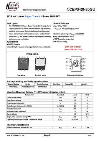
http //www.ncepower.com NCEP040N85GU NCE N-Channel Super Trench II Power MOSFET Description General Features The NCEP040N85GU uses Super Trench II technology that is V =85V,I =125A DS D uniquely optimized to provide the most efficient high frequency R =3.2m (typical) @ V =10V DS(ON) GS switching performance. Both conduction and switching power losses are minimized due to an extrem... See More ⇒
6.9. Size:400K ncepower
ncep040n12.pdf 

NCEP040N12, NCEP040N12D NCE N-Channel Super Trench II Power MOSFET Description General Features The series of devices uses Super Trench II technology that is VDS =120V,ID =150A uniquely optimized to provide the most efficient high frequency RDS(ON)=3.5m , typical (TO-220)@ VGS=10V switching performance. Both conduction and switching power RDS(ON)=3.3m , typical (TO-2... See More ⇒
6.10. Size:363K ncepower
ncep040n10m.pdf 

NCEP040N10M,NCEP040N10MD NCE N-Channel Super Trench II Power MOSFET Description General Features The series of devices uses Super Trench II technology that is VDS =100V,ID =130A uniquely optimized to provide the most efficient high frequency RDS(ON)=3.7m , typical (TO-220)@ VGS=10V switching performance. Both conduction and switching power RDS(ON)=3.55m , typical (TO-263)@ VG... See More ⇒
6.11. Size:1002K ncepower
ncep040n85m ncep040n85md.pdf 

Pb Free Product NCEP040N85M NCEP040N85MD NCE N-Channel Super Trench II Power MOSFET Description The series of devices uses Super Trench II technology that is General Features uniquely optimized to provide the most efficient high frequency V =85V,I =140A DS D switching performance. Both conduction and switching power R =3.4m , typical (TO-220)@ V =10V DS(ON) GS losses are minimi... See More ⇒
6.12. Size:325K ncepower
ncep040n85 ncep040n85d.pdf 

NCEP040N85, NCEP040N85D NCE N-Channel Super Trench II Power MOSFET Description The series of devices uses Super Trench II technology that is General Features uniquely optimized to provide the most efficient high frequency VDS =85V,ID =140A switching performance. Both conduction and switching power RDS(ON)=3.5m , typical (TO-220)@ VGS=10V losses are minimized due to an ext... See More ⇒
6.13. Size:699K ncepower
ncep040n85d.pdf 

NCEP040N85, NCEP040N85D NCE N-Channel Super Trench II Power MOSFET Description The series of devices uses Super Trench II technology that is General Features uniquely optimized to provide the most efficient high frequency V =85V,I =140A DS D switching performance. Both conduction and switching power R =3.5m , typical (TO-220)@ V =10V DS(ON) GS losses are minimized due to an extr... See More ⇒
6.14. Size:985K ncepower
ncep040n10gu.pdf 

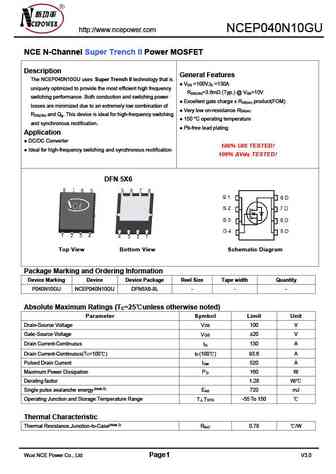
http //www.ncepower.com NCEP040N10GU NCE N-Channel Super Trench II Power MOSFET Description General Features The NCEP040N10GU uses Super Trench II technology that is V =100V,I =130A DS D uniquely optimized to provide the most efficient high frequency R =3.6m (Typ.) @ V =10V DS(ON) GS switching performance. Both conduction and switching power Excellent gate charge x R produc... See More ⇒
6.15. Size:363K ncepower
ncep040n10 ncep040n10d.pdf 

NCEP040N10,NCEP040N10D NCE N-Channel Super Trench II Power MOSFET Description General Features The series of devices uses Super Trench II technology that is VDS =100V,ID =130A uniquely optimized to provide the most efficient high frequency RDS(ON)=3.7m , typical (TO-220)@ VGS=10V switching performance. Both conduction and switching power RDS(ON)=3.55m , typical (TO-263)@ VGS=... See More ⇒
6.16. Size:400K ncepower
ncep040n12 ncep040n12d.pdf 

NCEP040N12, NCEP040N12D NCE N-Channel Super Trench II Power MOSFET Description General Features The series of devices uses Super Trench II technology that is VDS =120V,ID =150A uniquely optimized to provide the most efficient high frequency RDS(ON)=3.5m , typical (TO-220)@ VGS=10V switching performance. Both conduction and switching power RDS(ON)=3.3m , typical (TO-2... See More ⇒
Detailed specifications: NCEP040N10GU, NCEP040N10M, NCEP040N12, NCEP040N12D, NCEP040N85G, NCEP040N85GU, NCEP040N85M, NCEP040N85MD, IRF520, NCEP045N10AG, NCEP045N10F, NCEP045N10G, NCEP045N10M, NCEP045N85, NCEP045N85G, NCEP045N85GU, NCEP048N72
Keywords - NCEP040NH150LL MOSFET specs
NCEP040NH150LL cross reference
NCEP040NH150LL equivalent finder
NCEP040NH150LL pdf lookup
NCEP040NH150LL substitution
NCEP040NH150LL replacement
Can't find your MOSFET?
Learn how to find a substitute transistor by analyzing voltage, current and package compatibility
