NCEP055N10G Datasheet. Specs and Replacement
Type Designator: NCEP055N10G
Type of Transistor: MOSFET
Type of Control Channel: N-Channel
Absolute Maximum Ratings
Pd ⓘ - Maximum Power Dissipation: 120 W
|Vds|ⓘ - Maximum Drain-Source Voltage: 100 V
|Vgs|ⓘ - Maximum Gate-Source Voltage: 20 V
|Id| ⓘ - Maximum Drain Current: 105 A
Tj ⓘ - Maximum Junction Temperature: 150 °C
Electrical Characteristics
tr ⓘ - Rise Time: 12 nS
Cossⓘ - Output Capacitance: 400 pF
RDSonⓘ - Maximum Drain-Source On-State Resistance: 0.0055 Ohm
Package: DFN5X6-8L
NCEP055N10G substitution
- MOSFET ⓘ Cross-Reference Search
NCEP055N10G datasheet
ncep055n10g.pdf
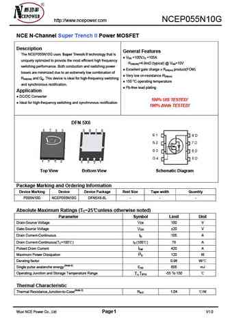
http //www.ncepower.com NCEP055N10G NCE N-Channel Super Trench II Power MOSFET Description General Features The NCEP055N10G uses Super Trench II technology that is VDS =100V,ID =105A uniquely optimized to provide the most efficient high frequency RDS(ON)=4.9m (typical) @ VGS=10V switching performance. Both conduction and switching power Excellent gate charge x RDS(on... See More ⇒
ncep055n10u.pdf
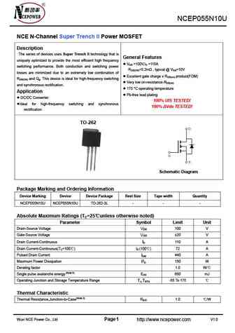
NCEP055N10U NCE N-Channel Super Trench II Power MOSFET Description The series of devices uses Super Trench II technology that is General Features uniquely optimized to provide the most efficient high frequency VDS =100V,ID =110A switching performance. Both conduction and switching power RDS(ON)=5.2m , typical @ VGS=10V losses are minimized due to an extremely low combin... See More ⇒
ncep055n10.pdf

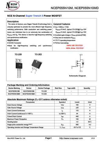
NCEP055N10, NCEP055N10D NCE N-Channel Super Trench II Power MOSFET Description The series of devices uses Super Trench II technology that is General Features uniquely optimized to provide the most efficient high frequency VDS =100V,ID =110A switching performance. Both conduction and switching power RDS(ON)=5.4m , typical (TO-220)@ VGS=10V losses are minimized due to an ex... See More ⇒
ncep055n10m.pdf
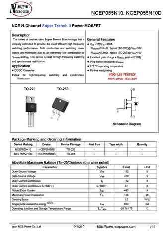
NCEP055N10M, NCEP055N10MD NCE N-Channel Super Trench II Power MOSFET Description The series of devices uses Super Trench II technology that is General Features uniquely optimized to provide the most efficient high frequency V =100V,I =110A DS D switching performance. Both conduction and switching power R =5.4m , typical (TO-220)@ V =10V DS(ON) GS losses are minimized due to an e... See More ⇒

Detailed specifications: NCEP050N12AGU, NCEP050N12D, NCEP050N12GU, NCEP050N85G, NCEP050N85M, NCEP053N85GU, NCEP055N10, NCEP055N10D, AO4468, NCEP055N10M, NCEP055N10U, NCEP055N12, NCEP055N12AG, NCEP055N12D, NCEP055N12G, NCEP055N30GU, NCEP055N60GU
Keywords - NCEP055N10G MOSFET specs
NCEP055N10G cross reference
NCEP055N10G equivalent finder
NCEP055N10G pdf lookup
NCEP055N10G substitution
NCEP055N10G replacement
Can't find your MOSFET? Learn how to find a substitute transistor by analyzing voltage, current and package compatibility
History: PHX9NQ20T
🌐 : EN ES РУ

LIST
Last Update
MOSFET: RM50P30DF | CRTT095N12N | CRSS028N10N | CRST030N10N | CRJQ80N65F | ASDM20N20KQ | ASDM20N100Q | ASDM12N65F | ASDM100R750PKQ | ASDM100R160NKQ
Popular searches
j5027-r datasheet | transistor a1015 datasheet | bf199 transistor equivalent | bu801 | c8550 transistor datasheet | mj21194 transistor datasheet | kep40n26 | nte103a