NCEP078N10AG Datasheet. Specs and Replacement
Type Designator: NCEP078N10AG
Type of Transistor: MOSFET
Type of Control Channel: N-Channel
Absolute Maximum Ratings
Pd ⓘ
- Maximum Power Dissipation: 100 W
|Vds|ⓘ - Maximum Drain-Source Voltage: 100 V
|Vgs|ⓘ - Maximum Gate-Source Voltage: 20 V
|Id| ⓘ - Maximum Drain Current: 75 A
Tj ⓘ - Maximum Junction Temperature: 150 °C
Electrical Characteristics
tr ⓘ - Rise Time: 11 nS
Cossⓘ -
Output Capacitance: 305 pF
RDSonⓘ - Maximum Drain-Source On-State Resistance: 0.0105 Ohm
Package: DFN5X6-8L
NCEP078N10AG substitution
- MOSFET ⓘ Cross-Reference Search
NCEP078N10AG datasheet
..1. Size:428K ncepower
ncep078n10ag.pdf 
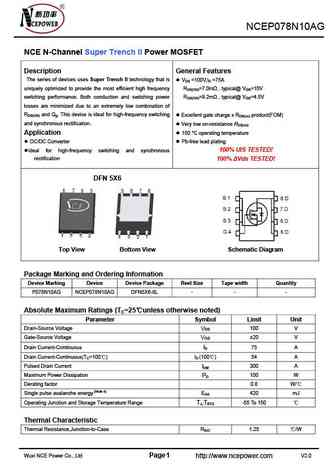
NCEP078N10AG NCE N-Channel Super Trench II Power MOSFET Description General Features The series of devices uses Super Trench II technology that is VDS =100V,ID =75A uniquely optimized to provide the most efficient high frequency RDS(ON)=7.0m , typical@ VGS=10V switching performance. Both conduction and switching power RDS(ON)=9.2m , typical@ VGS=4.5V losses are minimized... See More ⇒
3.1. Size:462K ncepower
ncep078n10ak.pdf
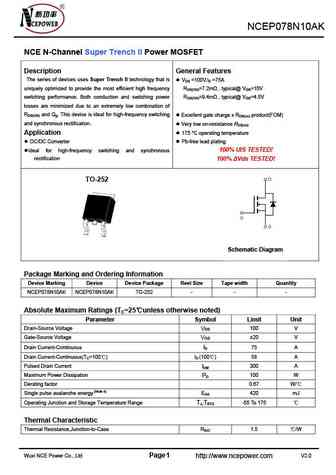
NCEP078N10AK NCE N-Channel Super Trench II Power MOSFET Description General Features The series of devices uses Super Trench II technology that is VDS =100V,ID =75A uniquely optimized to provide the most efficient high frequency RDS(ON)=7.2m , typical@ VGS=10V switching performance. Both conduction and switching power RDS(ON)=9.4m , typical@ VGS=4.5V losses are minimized... See More ⇒
4.1. Size:1009K ncepower
ncep078n10g.pdf
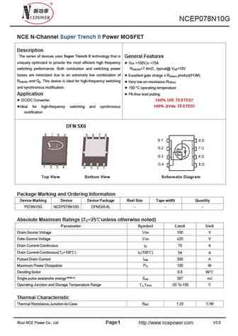
NCEP078N10G NCE N-Channel Super Trench II Power MOSFET Description The series of devices uses Super Trench II technology that is General Features uniquely optimized to provide the most efficient high frequency V =100V,I =75A DS D switching performance. Both conduction and switching power R =7.4m , typical@ V =10V DS(ON) GS losses are minimized due to an extremely low combination... See More ⇒
8.1. Size:331K ncepower
ncep075n85agu.pdf
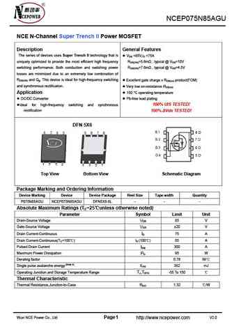
NCEP075N85AGU NCE N-Channel Super Trench II Power MOSFET Description General Features The series of devices uses Super Trench II technology that is VDS =85V,ID =75A uniquely optimized to provide the most efficient high frequency RDS(ON)=5.6m , typical @ VGS=10V switching performance. Both conduction and switching power RDS(ON)=7.6m , typical @ VGS=4.5V losses are minimiz... See More ⇒
8.2. Size:760K ncepower
ncep075n85gu.pdf
NCEP075N85GU NCE N-Channel Super Trench II Power MOSFET Description General Features The series of devices uses Super Trench II technology that is V =85V,I =75A DS D uniquely optimized to provide the most efficient high frequency R =5.6m , typical @ V =10V DS(ON) GS switching performance. Both conduction and switching power losses are minimized due to an extremely low combinati... See More ⇒
8.3. Size:305K ncepower
ncep072n10.pdf
http //www.ncepower.com NCEP072N10 NCE N-Channel Super Trench II Power MOSFET Description General Features The NCEP072N10 uses Super Trench II technology that is VDS =100V,ID =90A uniquely optimized to provide the most efficient high frequency RDS(ON)=6.8m (typical) @ VGS=10V switching performance. Both conduction and switching power Excellent gate charge x RDS(on) p... See More ⇒
8.4. Size:397K ncepower
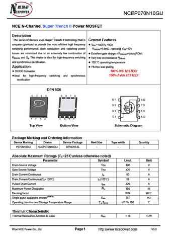
ncep070n10agu.pdf

NCEP070N10AGU NCE N-Channel Super Trench II Power MOSFET Description General Features The series of devices uses Super Trench II technology that is VDS =100V,ID =80A uniquely optimized to provide the most efficient high frequency RDS(ON)=6.1m , typical@ VGS=10V switching performance. Both conduction and switching power RDS(ON)=8.35m , typical@ VGS=4.5V losses are minimiz... See More ⇒
8.5. Size:335K ncepower
ncep070n12.pdf

NCEP070N12,NCEP070N12D NCE N-Channel Super Trench II Power MOSFET Description General Features The series of devices uses Super Trench II technology that is VDS =120V,ID =100A uniquely optimized to provide the most efficient high frequency RDS(ON)=6.5m , typical (TO-220)@ VGS=10V switching performance. Both conduction and switching power RDS(ON)=6.3m , typical (TO-26... See More ⇒
8.6. Size:335K ncepower
ncep070n12 ncep070n12d.pdf

NCEP070N12,NCEP070N12D NCE N-Channel Super Trench II Power MOSFET Description General Features The series of devices uses Super Trench II technology that is VDS =120V,ID =100A uniquely optimized to provide the most efficient high frequency RDS(ON)=6.5m , typical (TO-220)@ VGS=10V switching performance. Both conduction and switching power RDS(ON)=6.3m , typical (TO-26... See More ⇒
8.7. Size:335K ncepower
ncep070n12d.pdf
NCEP070N12,NCEP070N12D NCE N-Channel Super Trench II Power MOSFET Description General Features The series of devices uses Super Trench II technology that is VDS =120V,ID =100A uniquely optimized to provide the most efficient high frequency RDS(ON)=6.5m , typical (TO-220)@ VGS=10V switching performance. Both conduction and switching power RDS(ON)=6.3m , typical (TO-26... See More ⇒
8.8. Size:627K ncepower
ncep072n10a.pdf
http //www.ncepower.com NCEP072N10A NCE N-Channel Super Trench II Power MOSFET Description General Features The NCEP072N10A uses Super Trench II technology that is V =100V,I =88A DS D uniquely optimized to provide the most efficient high frequency R =6.2m (typical) @ V =10V DS(ON) GS switching performance. Both conduction and switching power R =8.4m (typical) @ V =4.5V DS(ON) GS... See More ⇒
8.9. Size:377K ncepower
ncep070n10gu.pdf
NCEP070N10GU NCE N-Channel Super Trench II Power MOSFET Description The series of devices uses Super Trench II technology that is General Features uniquely optimized to provide the most efficient high frequency VDS =100V,ID =80A switching performance. Both conduction and switching power RDS(ON)=6.6m , typical@ VGS=10V losses are minimized due to an extremely low combinati... See More ⇒
Detailed specifications: NCEP068N10K, NCEP070N10AGU, NCEP070N10GU, NCEP070N12, NCEP070N12D, NCEP072N10A, NCEP075N85AGU, NCEP075N85GU, 2N7002, NCEP078N10AK, NCEP078N10G, NCEP080N10, NCEP080N10A, NCEP080N10F, NCEP080N12, NCEP080N12D, NCEP080N12G
Keywords - NCEP078N10AG MOSFET specs
NCEP078N10AG cross reference
NCEP078N10AG equivalent finder
NCEP078N10AG pdf lookup
NCEP078N10AG substitution
NCEP078N10AG replacement
Learn how to find the right MOSFET substitute. A guide to cross-reference, check specs and replace MOSFETs in your circuits.
