FIR2N60AFG Specs and Replacement
Type Designator: FIR2N60AFG
Type of Transistor: MOSFET
Type of Control Channel: N-Channel
Absolute Maximum Ratings
Pd ⓘ - Maximum Power Dissipation: 35 W
|Vds|ⓘ - Maximum Drain-Source Voltage: 600 V
|Vgs|ⓘ - Maximum Gate-Source Voltage: 30 V
|Id| ⓘ - Maximum Drain Current: 2 A
Tj ⓘ - Maximum Junction Temperature: 150 °C
Electrical Characteristics
tr ⓘ - Rise Time: 5.5 nS
Cossⓘ - Output Capacitance: 30 pF
RDSonⓘ - Maximum Drain-Source On-State Resistance: 4.5 Ohm
Package: TO-220F
FIR2N60AFG substitution
- MOSFET ⓘ Cross-Reference Search
FIR2N60AFG datasheet
fir2n60afg.pdf
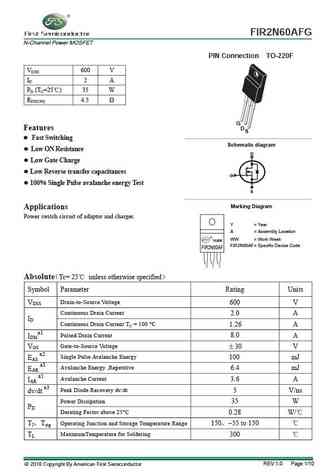
FIR2N60AFG N-Channel Power MOSFET PIN Connection TO-220F VDSS 600 V ID 2 A PD (TC=25 ) 35 W RDS(ON) 4.5 G Features D S Fast Switching g Schematic dia ram Low ON Resistance D Low Gate Charge Low Reverse transfer capacitances G 100% Single Pulse avalanche energy Test S Marking Diagram Applications Power switch circuit of adaptor and charger. Y = Year ... See More ⇒
fir2n60alg.pdf
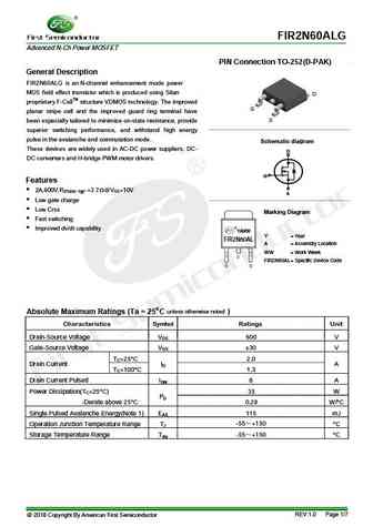
FIR2N60ALG Advanced N-Ch Power MOSFET PIN Connection TO-252(D-PAK) General Description FIR2N60ALG is an N-channel enhancement mode power MOS field effect transistor which is produced using Silan D proprietary F-CellTM structure VDMOS technology. The improved G planar stripe cell and the improved guard ring terminal have been especially tailored to minimize on-state resistance, prov... See More ⇒
fir2n65afg.pdf
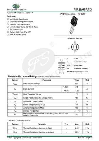
FIR2N65AFG Advanced N-Ch Power MOSFET-X PIN Connection TO-220F Features Low Intrinsic Capacitances. Excellent Switching Characteristics. Extended Safe Operating Area. Unrivalled Gate Charge Qg=6.5nC (Typ.). BVDSS=650V,ID=2A G RDS(on) 4.2 (Typ) @VG=10V DS 100% Avalanche Tested g Schematic dia ram D G S Y = Year A = Assembly Location WW = Wor... See More ⇒
fir2n65abpg.pdf
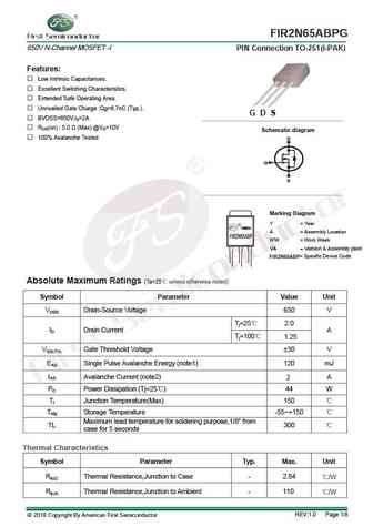
FIR2N65ABPG FIR2N65ABPG 650V N-Channel MOSFET -I PIN Connection TO-251(I-PAK) Features Low Intrinsic Capacitances. Excellent Switching Characteristics. Extended Safe Operating Area. Unrivalled Gate Charge Qg=6.7nC (Typ.). G D S BVDSS=650V,ID=2A RDS(on) 5.0 (Max) @VG=10V g Schematic dia ram 100% Avalanche Tested D G S Marking Diagram Y... See More ⇒
Detailed specifications: FIR20N10LG, FIR20N15LG, FIR20N50FG, FIR20N60FG, FIR20N65FG, FIR20NS65AFG, FIR24N50APTG, FIR25N03D3G, K3569, FIR2N65AFG, FIR2N70FG, FIR2N80FG, FIR30N03D3G, FIR40N10LG, FIR40N15LG, FIR40N20LG, FIR4N70FG
Keywords - FIR2N60AFG MOSFET specs
FIR2N60AFG cross reference
FIR2N60AFG equivalent finder
FIR2N60AFG pdf lookup
FIR2N60AFG substitution
FIR2N60AFG replacement
Need a MOSFET replacement? Our guide shows you how to find a perfect substitute by comparing key parameters and specs
🌐 : EN ES РУ

LIST
Last Update
MOSFET: CM4407 | CM3407 | CM3400 | SVF11N65F | SVF11N65T | FKBB3105 | EHBA036R1 | CRTT067N10N | AP6NA3R2MT | AP65SA145DDT8
Popular searches
2sc1345 | 2sd555 | a950 transistor | k2611 | c1740 transistor | c828 transistor | c4467 | c2383 transistor