P1560JD Datasheet. Specs and Replacement
Type Designator: P1560JD 📄📄
Type of Transistor: MOSFET
Type of Control Channel: N-Channel
Absolute Maximum Ratings
Pd ⓘ - Maximum Power Dissipation: 96 W
|Vds|ⓘ - Maximum Drain-Source Voltage: 600 V
|Vgs|ⓘ - Maximum Gate-Source Voltage: 30 V
|Id| ⓘ - Maximum Drain Current: 15 A
Tj ⓘ - Maximum Junction Temperature: 150 °C
Electrical Characteristics
|VGSth|ⓘ - Maximum Gate-Threshold Voltage: 4 V
Qg ⓘ - Total Gate Charge: 26 nC
tr ⓘ - Rise Time: 35 nS
Cossⓘ - Output Capacitance: 47 pF
RDSonⓘ - Maximum Drain-Source On-State Resistance: 0.31 Ohm
Package: TO-252
P1560JD substitution
- MOSFET ⓘ Cross-Reference Search
P1560JD datasheet
p1560jd.pdf
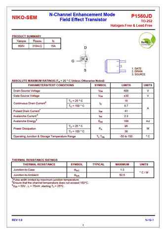
N-Channel Enhancement Mode P1560JD NIKO-SEM Field Effect Transistor TO-252 Halogen-Free & Lead-Free PRODUCT SUMMARY V(BR)DSS RDS(ON) ID 600V 310m 15A D G 1. GATE S 2. DRAIN 3. SOURCE ABSOLUTE MAXIMUM RATINGS (TA = 25 C Unless Otherwise Noted) PARAMETERS/TEST CONDITIONS SYMBOL LIMITS UNITS Drain-Source Voltage VDS 600 V Gate-Source Voltage VGS 30 V TC ... See More ⇒
p1560jf.pdf
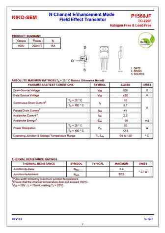
N-Channel Enhancement Mode P1560JF NIKO-SEM Field Effect Transistor TO-220F Halogen-Free & Lead-Free PRODUCT SUMMARY V(BR)DSS RDS(ON) ID 600V 290m 15A D G 1. GATE S 2. DRAIN 3. SOURCE ABSOLUTE MAXIMUM RATINGS (TA = 25 C Unless Otherwise Noted) PARAMETERS/TEST CONDITIONS SYMBOL LIMITS UNITS Drain-Source Voltage VDS 600 V Gate-Source Voltage VGS 30 V TC... See More ⇒
Detailed specifications: P1165JD, P1165JFN, P1306ED, P1306EK, P1350ETF, P1406BV, P1410BD, P1410BK, 20N50, P1560JF, P1610AK, P1610ATF, P1615ATA, P1615ATFA, P1625ED, P1850EF, P2020YD
Keywords - P1560JD MOSFET specs
P1560JD cross reference
P1560JD equivalent finder
P1560JD pdf lookup
P1560JD substitution
P1560JD replacement
Need a MOSFET replacement? Our guide shows you how to find a perfect substitute by comparing key parameters and specs
🌐 : EN ES РУ

LIST
Last Update
MOSFET: ASDM30P100KQ | ASDM30N90Q | ASDM30N75KQ | ASDM30N150Q | ASDM30N120Q | ASDM30N120KQ | ASDM30N100KQ | ASDM30DN40E | ASDM30DN30E | ASDM3050KQ
Popular searches
transistor 2222a | 8050 transistor | bc238 | 2sb772 | 2n2222a-1726 datasheet | bc516 | 2n3391 equivalent | a562 transistor