PV555BA Specs and Replacement
Type Designator: PV555BA
Type of Transistor: MOSFET
Type of Control Channel: P-Channel
Absolute Maximum Ratings
Pd ⓘ - Maximum Power Dissipation: 1.7 W
|Vds|ⓘ - Maximum Drain-Source Voltage: 30 V
|Vgs|ⓘ - Maximum Gate-Source Voltage: 20 V
|Id| ⓘ - Maximum Drain Current: 6 A
Tj ⓘ - Maximum Junction Temperature: 150 °C
Electrical Characteristics
tr ⓘ - Rise Time: 7.8 nS
Cossⓘ - Output Capacitance: 120 pF
RDSonⓘ - Maximum Drain-Source On-State Resistance: 0.028 Ohm
Package: SOP-8
PV555BA substitution
- MOSFET ⓘ Cross-Reference Search
PV555BA datasheet
pv555ba.pdf
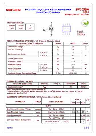
P-Channel Logic Level Enhancement Mode PV555BA NIKO-SEM SOP-8 Field Effect Transistor Halogen-free & Lead-Free D PRODUCT SUMMARY V(BR)DSS RDS(ON) ID 28m -6A -30V G G GATE D DRAIN S SOURCE S ABSOLUTE MAXIMUM RATINGS (TA = 25 C Unless Otherwise Noted) PARAMETERS/TEST CONDITIONS SYMBOL LIMITS UNITS Drain-Source Voltage VDS -30 V Gate-Source Voltage VGS 20... See More ⇒
Detailed specifications: PQ6V2JN, PQ6X6JN, PR802BA33, PR812BA33, PT5B9BA, PT676BA, PT6J6BA, PV521BA, 7N65, PV561BA, PV563BA, PV5G3EA, PV609CA, PV616DA, PV6A4BA, PV6A6BA, PV6A8BA
Keywords - PV555BA MOSFET specs
PV555BA cross reference
PV555BA equivalent finder
PV555BA pdf lookup
PV555BA substitution
PV555BA replacement
Need a MOSFET replacement? Our guide shows you how to find a perfect substitute by comparing key parameters and specs
🌐 : EN ES РУ

LIST
Last Update
MOSFET: AUW033N08BG | AUW025N10 | AUR030N10 | AUR020N10 | AUR020N085 | AUR014N10 | AUP074N10 | AUP065N10 | AUP062N08BG | AUP060N08AG
Popular searches
cs7n60f | d613 transistor | fdmc8884 mosfet | k3569 mosfet equivalent | 2sa1370 | 4508nh mosfet | a94 transistor | c5149 datasheet