PV6D2DA Specs and Replacement
Type Designator: PV6D2DA
Type of Transistor: MOSFET
Type of Control Channel: N-Channel
Absolute Maximum Ratings
Pd ⓘ - Maximum Power Dissipation: 2.1 W
|Vds|ⓘ - Maximum Drain-Source Voltage: 40 V
|Vgs|ⓘ - Maximum Gate-Source Voltage: 20 V
|Id| ⓘ - Maximum Drain Current: 6.4 A
Tj ⓘ - Maximum Junction Temperature: 150 °C
Electrical Characteristics
tr ⓘ - Rise Time: 79 nS
Cossⓘ - Output Capacitance: 62 pF
RDSonⓘ - Maximum Drain-Source On-State Resistance: 0.025 Ohm
Package: SOP-8
PV6D2DA substitution
- MOSFET ⓘ Cross-Reference Search
PV6D2DA datasheet
pv6d2da.pdf
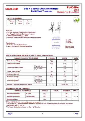
PV6D2DA Dual N-Channel Enhancement Mode NIKO-SEM SOP-8 Field Effect Transistor Halogen-Free & Lead-Free PRODUCT SUMMARY V(BR)DSS RDS(ON) ID 40V 25m 6.4A Features Pb-Free, Halogen Free and RoHS compliant. Low RDS(on) to Minimize Conduction Losses. Ohmic Region Good RDS(on) Ratio. Optimized Gate Charge to Minimize Switching Losses. G GATE D DRA... See More ⇒
Detailed specifications: PV561BA, PV563BA, PV5G3EA, PV609CA, PV616DA, PV6A4BA, PV6A6BA, PV6A8BA, IRF4905, PW567EA, PW5D8EA, PW5S6EA, PX567EA, PX567JZ, PX5D8EA, PX5D8JZ-T, PX5S6EA
Keywords - PV6D2DA MOSFET specs
PV6D2DA cross reference
PV6D2DA equivalent finder
PV6D2DA pdf lookup
PV6D2DA substitution
PV6D2DA replacement
Can't find your MOSFET? Learn how to find a substitute transistor by analyzing voltage, current and package compatibility
🌐 : EN ES РУ

LIST
Last Update
MOSFET: AUW033N08BG | AUW025N10 | AUR030N10 | AUR020N10 | AUR020N085 | AUR014N10 | AUP074N10 | AUP065N10 | AUP062N08BG | AUP060N08AG
Popular searches
pkch2bb mosfet | 2024ont | 2n1306 transistor | 2sa750 datasheet | 2sa940 transistor datasheet | 2sb549 | 5n50 mosfet equivalent | a1016 transistor