630 Datasheet. Specs and Replacement
Type Designator: 630 📄📄
Type of Transistor: MOSFET
Type of Control Channel: N-Channel
Absolute Maximum Ratings
Pd ⓘ - Maximum Power Dissipation: 75 W
|Vds|ⓘ - Maximum Drain-Source Voltage: 200 V
|Vgs|ⓘ - Maximum Gate-Source Voltage: 30 V
|Id| ⓘ - Maximum Drain Current: 9 A
Tj ⓘ - Maximum Junction Temperature: 150 °C
Electrical Characteristics
tr ⓘ - Rise Time: 3.5 nS
Cossⓘ - Output Capacitance: 94 pF
RDSonⓘ - Maximum Drain-Source On-State Resistance: 0.28 Ohm
Package: TO220
📄📄 Copy
630 substitution
- MOSFET ⓘ Cross-Reference Search
630 datasheet
630 f630 i630 e630 b630 d630.pdf
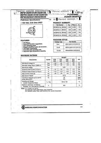
630/F630/I630/ E630/B630/D630 9A 200V N-channel Enhancement Mode Power MOSFET 1 Description These N-channel enhanced vdmosfets, is obtained by the 2 D V = 200V self-aligned planar technology which reduce the conduction DSS loss, improve switching performance and enhance the R = 0.23 DS(on) (TYP) G avalanche energy. Which accords with the RoHS standard. 1 I = 9A 3 S D 2 Feature... See More ⇒
irlhm630trpbf.pdf
IRLHM630PbF HEXFET Power MOSFET VDSS 30 V VGS 12 V RDS(on) max 3.5 (@ VGS = 4.5V) m (@ VGS = 2.5V) 4.5 Qg (typical) 41 nC ID 40 A PQFN 3.3 x 3.3 mm (@TC (Bottom) = 25 C) Applications Battery Operated DC Motor Inverter MOSFET Secondary Side Synchronous Rectification MOSFET Features Benefits Low RDSon (... See More ⇒
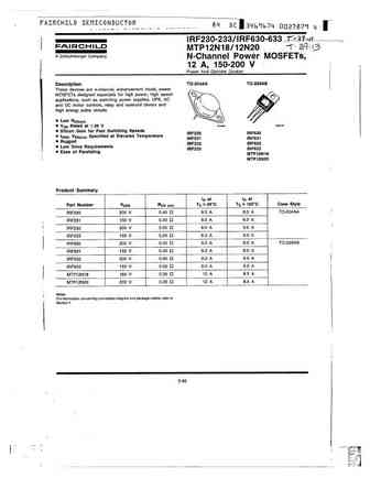
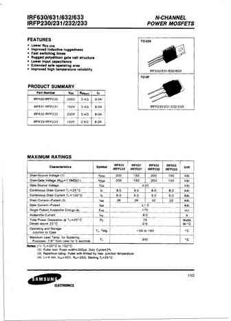
irf630 irf631 irf632 irf633 irf230 irf231 irf232 irf233 mtp12n18 mtp12n20.pdf

... See More ⇒
irf630b irfs630b.pdf

IRF630B/IRFS630B 200V N-Channel MOSFET General Description Features These N-Channel enhancement mode power field effect 9.0A, 200V, RDS(on) = 0.4 @VGS = 10 V transistors are produced using Fairchild s proprietary, Low gate charge ( typical 22 nC) planar, DMOS technology. Low Crss ( typical 22 pF) This advanced technology has been especially tailored to Fast switchin... See More ⇒
2n5630 2n6030 2n5631 2n6031.pdf
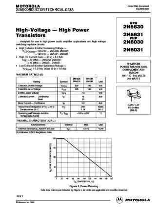
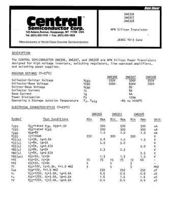
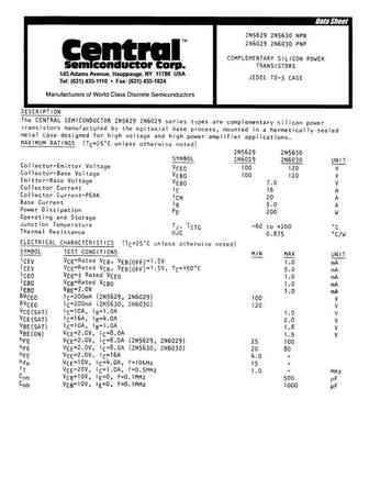
Order this document MOTOROLA by 2N5630/D SEMICONDUCTOR TECHNICAL DATA NPN 2N5630 High-Voltage High Power 2N5631 Transistors PNP . . . designed for use in high power audio amplifier applications and high voltage 2N6030 switching regulator circuits. High Collector Emitter Sustaining Voltage 2N6031 VCEO(sus) = 120 Vdc 2N5630, 2N6030 VCEO(sus) = 140 Vdc 2N5631, 2N603... See More ⇒
irl630s.pdf
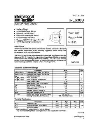
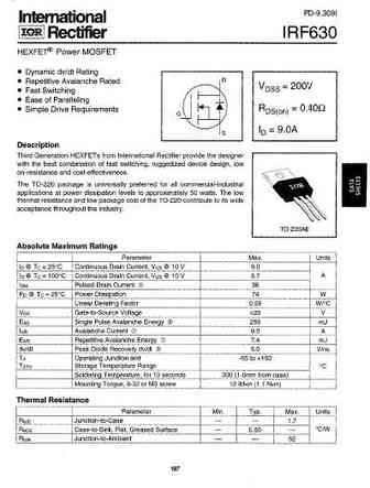
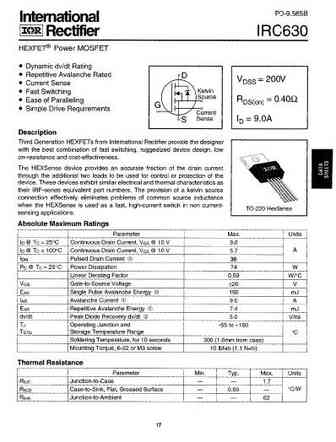
PD - 9.1254 IRL630S HEXFET Power MOSFET Surface Mount Available in Tape & Reel VDSS = 200V Dynamic dv/dt Rating Repetitive Avalanche Rated RDS(on) = 0.40 Logic-Level Gate Drive RDS(ON) Specified at VGS = 4V & 5V 150 C Operating Temperature ID = 9.0A Description Third Generation HEXFETs from International Rectifier provide the designer with the best combination of fast switc... See More ⇒
irf630npbf irf630nspbf irf630nlpbf.pdf

PD - 95047A IRF630NPbF IRF630NSPbF l Advanced Process Technology IRF630NLPbF l Dynamic dv/dt Rating HEXFET Power MOSFET l 175 C Operating Temperature l Fast Switching D VDSS = 200V l Fully Avalanche Rated l Ease of Paralleling l Simple Drive Requirements RDS(on) = 0.30 G l Lead-Free Description ID = 9.3A Fifth Generation HEXFET Power MOSFETs from S International Rec... See More ⇒
irl630pbf.pdf
PD- 95756 IRL630PbF Lead-Free 8/24/04 Document Number 91303 www.vishay.com 1 IRL630PbF Document Number 91303 www.vishay.com 2 IRL630PbF Document Number 91303 www.vishay.com 3 IRL630PbF Document Number 91303 www.vishay.com 4 IRL630PbF Document Number 91303 www.vishay.com 5 IRL630PbF Document Number 91303 www.vishay.com 6 IRL630PbF Document Number 91303 www.... See More ⇒
irlhm630pbf.pdf
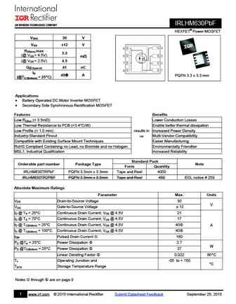
IRLHM630PbF HEXFET Power MOSFET VDSS 30 V VGS 12 V RDS(on) max 3.5 (@ VGS = 4.5V) m (@ VGS = 2.5V) 4.5 Qg (typical) 41 nC ID 40 A PQFN 3.3 x 3.3 mm (@TC (Bottom) = 25 C) Applications Battery Operated DC Motor Inverter MOSFET Secondary Side Synchronous Rectification MOSFET Features Benefits Low RDSon (... See More ⇒
irlml6302gpbf.pdf
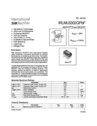
PD - 96159 IRLML6302GPbF HEXFET Power MOSFET l Generation V Technology l Ultra Low On-Resistance l P-Channel MOSFET VDSS = -20V l SOT-23 Footprint l Low Profile (... See More ⇒
irfi630g.pdf
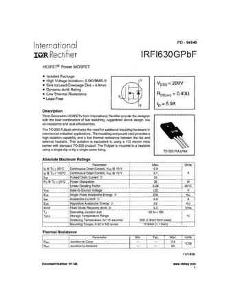
PD - 94846 IRFI630GPbF Lead-Free 11/14/03 Document Number 91148 www.vishay.com 1 IRFI630GPbF Document Number 91148 www.vishay.com 2 IRFI630GPbF Document Number 91148 www.vishay.com 3 IRFI630GPbF Document Number 91148 www.vishay.com 4 IRFI630GPbF Document Number 91148 www.vishay.com 5 IRFI630GPbF Document Number 91148 www.vishay.com 6 IRFI630GPbF TO-220 Full... See More ⇒
irlml6302pbf.pdf
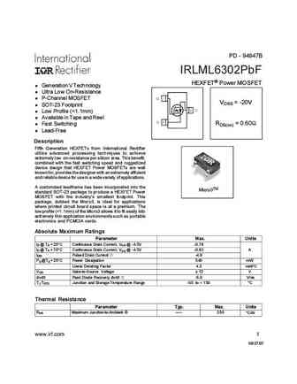
PD - 94947B IRLML6302PbF HEXFET Power MOSFET l Generation V Technology l Ultra Low On-Resistance l P-Channel MOSFET VDSS = -20V l SOT-23 Footprint l Low Profile (... See More ⇒
irlml6302.pdf
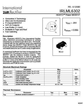
PD - 9.1259D IRLML6302 HEXFET Power MOSFET Generation V Technology D Ultra Low On-Resistance P-Channel MOSFET VDSS = -20V SOT-23 Footprint Low Profile (... See More ⇒
irgs4630d.pdf
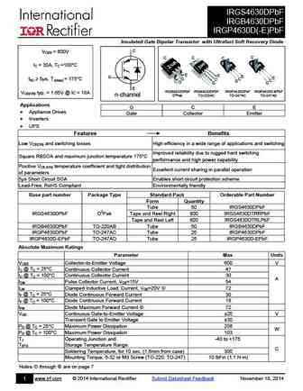
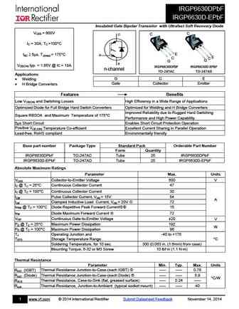
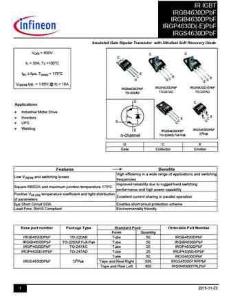
IRGS4630DPbF IRGB4630DPbF IRGP4630D(-E)PbF Insulated Gate Bipolar Transistor with Ultrafast Soft Recovery Diode C VCES = 600V C C C C IC = 30A, TC =100 C E E E G E C tSC 5 s, TJ(max) = 175 C C C C G G G G E IRGS4630DPbF IRGB4630DPbF IRGP4630D-EPbF IRGP4630DPbF VCE(ON) typ. = 1.65V @ IC = 18A TO-220AC TO-247AD n-channel D2Pak TO-247AC Appl... See More ⇒
irf9630spbf.pdf
PD- 95771 IRF9630SPbF Lead-Free 06/06/05 Document Number 91085 www.vishay.com 1 IRF9630SPbF Document Number 91085 www.vishay.com 2 IRF9630SPbF Document Number 91085 www.vishay.com 3 IRF9630SPbF Document Number 91085 www.vishay.com 4 IRF9630SPbF Document Number 91085 www.vishay.com 5 IRF9630SPbF Document Number 91085 www.vishay.com 6 IRF9630SPbF Peak Diode R... See More ⇒
irl630.pdf
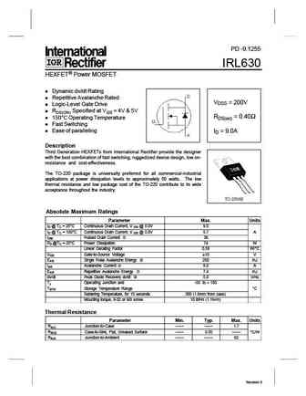
PD -9.1255 IRL630 HEXFET Power MOSFET Dynamic dv/dt Rating Repetitive Avalanche Rated VDSS = 200V Logic-Level Gate Drive RDS(ON) Specified at VGS = 4V & 5V RDS(on) = 0.40 150 C Operating Temperature Fast Switching Ease of paralleling ID = 9.0A Description Third Generation HEXFETs from International Rectifier provide the designer with the best combination of fast switching, ... See More ⇒
irc630pbf.pdf
PD- 96003B IRC630PbF Lead-Free www.irf.com 1 2/10/05 IRC630PbF 2 www.irf.com IRC630PbF www.irf.com 3 IRC630PbF 4 www.irf.com IRC630PbF www.irf.com 5 IRC630PbF 6 www.irf.com IRC630PbF www.irf.com 7 IRC630PbF 8 www.irf.com IRC630PbF HexsenseTO-220 5L Package Outline ( Dimensions are shown in millimeters (inches) Hexsense TO-220 5L Part Marking Information EXAMP... See More ⇒
irf630nlpbf irf630npbf irf630nspbf irf630nstrrpbf.pdf
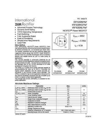
PD - 95047A IRF630NPbF IRF630NSPbF l Advanced Process Technology IRF630NLPbF l Dynamic dv/dt Rating HEXFET Power MOSFET l 175 C Operating Temperature l Fast Switching D VDSS = 200V l Fully Avalanche Rated l Ease of Paralleling l Simple Drive Requirements RDS(on) = 0.30 G l Lead-Free Description ID = 9.3A Fifth Generation HEXFET Power MOSFETs from S International Rec... See More ⇒
irli630gpbf.pdf
PD- 95653 IRLI630GPbF Lead-Free www.irf.com 1 7/26/04 IRLI630GPbF 2 www.irf.com IRLI630GPbF www.irf.com 3 IRLI630GPbF 4 www.irf.com IRLI630GPbF www.irf.com 5 IRLI630GPbF 6 www.irf.com IRLI630GPbF Peak Diode Recovery dv/dt Test Circuit + Circuit Layout Considerations Low Stray Inductance Ground Plane Low Leakage Inductance Current Transformer - + ... See More ⇒
irf630spbf.pdf
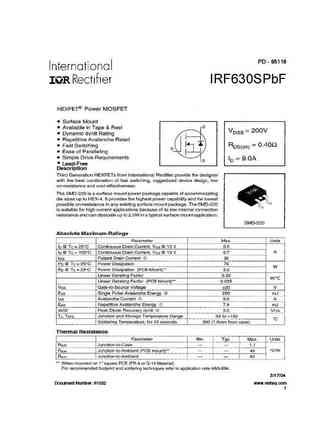
PD - 95118 IRF630SPbF Lead-Free 3/17/04 Document Number 91032 www.vishay.com 1 IRF630SPbF Document Number 91032 www.vishay.com 2 IRF630SPbF Document Number 91032 www.vishay.com 3 IRF630SPbF Document Number 91032 www.vishay.com 4 IRF630SPbF Document Number 91032 www.vishay.com 5 IRF630SPbF Document Number 91032 www.vishay.com 6 IRF630SPbF D2Pak Package Outli... See More ⇒
irli630g.pdf
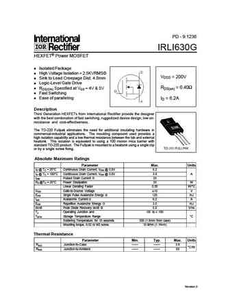
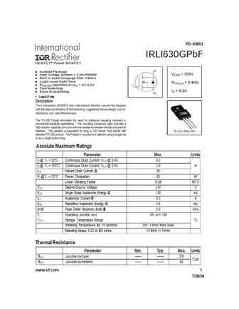
PD - 9.1236 IRLI630G HEXFET Power MOSFET Isolated Package High Voltage Isolation = 2.5KVRMS VDSS = 200V Sink to Lead Creepage Dist. 4.8mm Logic-Level Gate Drive RDS(on) = 0.40 RDS(ON) Specified at VGS = 4V & 5V Fast Switching Ease of paralleling ID = 6.2A Description Third Generation HEXFETs from International Rectifier provide the designer with the best combination of fast... See More ⇒
irfi9630g.pdf
PD - 94851 IRFI9630GPbF Lead-Free 11/07/03 Document Number 91167 www.vishay.com 1 IRFI9630GPbF Document Number 91167 www.vishay.com 2 IRFI9630GPbF Document Number 91167 www.vishay.com 3 IRFI9630GPbF Document Number 91167 www.vishay.com 4 IRFI9630GPbF Document Number 91167 www.vishay.com 5 IRFI9630GPbF Document Number 91167 www.vishay.com 6 IRFI9630GPbF TO-2... See More ⇒
irgp6630d.pdf
IRGP6630DPbF IRGP6630D-EPbF Insulated Gate Bipolar Transistor with Ultrafast Soft Recovery Diode VCES = 600V C C C IC = 30A, TC =100 C E tSC 5 s, TJ(max) = 175 C G E C G C G E VCE(ON) typ. = 1.65V @ IC = 18A IRGP6630DPbF IRGP6630D EPbF n-channel TO 247AC TO 247AD Applications G C E Welding Gate Collector Emitter H Bridg... See More ⇒
irf630n.pdf
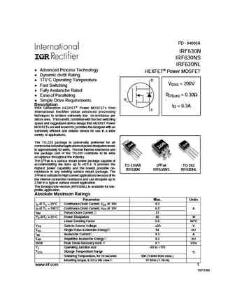
PD - 94005A IRF630N IRF630NS IRF630NL Advanced Process Technology HEXFET Power MOSFET Dynamic dv/dt Rating 175 C Operating Temperature D VDSS = 200V Fast Switching Fully Avalanche Rated RDS(on) = 0.30 Ease of Paralleling G Simple Drive Requirements Description ID = 9.3A Fifth Generation HEXFET Power MOSFETs from S International Rectifier utilize advanced proces... See More ⇒
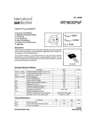
irf9630pbf.pdf
PD - 94958 IRF9630PbF Lead-Free 01/29/04 Document Number 91084 www.vishay.com 1 IRF9630PbF Document Number 91084 www.vishay.com 2 IRF9630PbF Document Number 91084 www.vishay.com 3 IRF9630PbF Document Number 91084 www.vishay.com 4 IRF9630PbF Document Number 91084 www.vishay.com 5 IRF9630PbF Document Number 91084 www.vishay.com 6 IRF9630PbF TO-220AB Package O... See More ⇒
irgb4630d.pdf

IRGS4630DPbF IRGB4630DPbF IRGP4630D(-E)PbF Insulated Gate Bipolar Transistor with Ultrafast Soft Recovery Diode C VCES = 600V C C C C IC = 30A, TC =100 C E E E G E C tSC 5 s, TJ(max) = 175 C C C C G G G G E IRGS4630DPbF IRGB4630DPbF IRGP4630D-EPbF IRGP4630DPbF VCE(ON) typ. = 1.65V @ IC = 18A TO-220AC TO-247AD n-channel D2Pak TO-247AC Appl... See More ⇒
irgp4630d.pdf

IRGS4630DPbF IRGB4630DPbF IRGP4630D(-E)PbF Insulated Gate Bipolar Transistor with Ultrafast Soft Recovery Diode C VCES = 600V C C C C IC = 30A, TC =100 C E E E G E C tSC 5 s, TJ(max) = 175 C C C C G G G G E IRGS4630DPbF IRGB4630DPbF IRGP4630D-EPbF IRGP4630DPbF VCE(ON) typ. = 1.65V @ IC = 18A TO-220AC TO-247AD n-channel D2Pak TO-247AC Appl... See More ⇒
irf630pbf.pdf
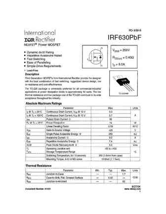
PD- 95916 IRF630PbF Lead-Free 9/27/04 Document Number 91031 www.vishay.com 1 IRF630PbF Document Number 91031 www.vishay.com 2 IRF630PbF Document Number 91031 www.vishay.com 3 IRF630PbF Document Number 91031 www.vishay.com 4 IRF630PbF Document Number 91031 www.vishay.com 5 IRF630PbF Document Number 91031 www.vishay.com 6 IRF630PbF Peak Diode Recovery dv/dt T... See More ⇒
irlml6302pbf-1.pdf
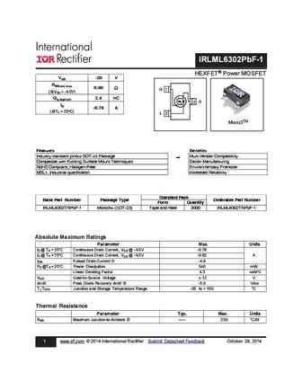
IRLML6302PbF-1 HEXFET Power MOSFET VDS -20 V RDS(on) max 0.60 G 1 (@V = -4.5V) GS Qg (typical) 2.4 nC 3 D ID -0.78 A (@T = 25 C) A S 2 Micro3TM Features Benefits Industry-standard pinout SOT-23 Package Multi-Vendor Compatibility Compatible with Existing Surface Mount Techniques Easier Manufacturing RoHS Compliant, Halogen-Free Environmentally Friendlier MSL1, In... See More ⇒
pbss5630pa.pdf
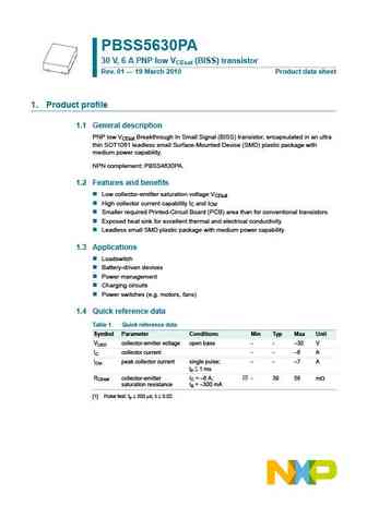
PBSS5630PA 30 V, 6 A PNP low VCEsat (BISS) transistor Rev. 01 19 March 2010 Product data sheet 1. Product profile 1.1 General description PNP low VCEsat Breakthrough In Small Signal (BISS) transistor, encapsulated in an ultra thin SOT1061 leadless small Surface-Mounted Device (SMD) plastic package with medium power capability. NPN complement PBSS4630PA. 1.2 Features and benefits... See More ⇒
irf630 s 1.pdf
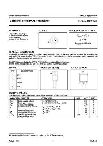
Philips Semiconductors Product specification N-channel TrenchMOS transistor IRF630, IRF630S FEATURES SYMBOL QUICK REFERENCE DATA Trench technology d Low on-state resistance VDSS = 200 V Fast switching Low thermal resistance ID = 9 A g RDS(ON) 400 m s GENERAL DESCRIPTION N-channel, enhancement mode field-effect power transistor using Trench technology... See More ⇒
pbss4630pa.pdf
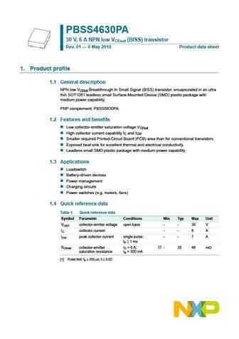
PBSS4630PA 30 V, 6 A NPN low VCEsat (BISS) transistor Rev. 01 6 May 2010 Product data sheet 1. Product profile 1.1 General description NPN low VCEsat Breakthrough In Small Signal (BISS) transistor, encapsulated in an ultra thin SOT1061 leadless small Surface-Mounted Device (SMD) plastic package with medium power capability. PNP complement PBSS5630PA. 1.2 Features and benefits ... See More ⇒
bfu630f.pdf
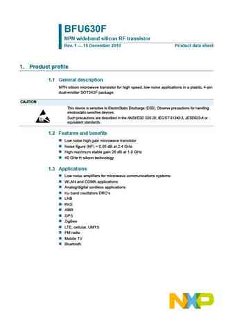
BFU630F NPN wideband silicon RF transistor Rev. 1 15 December 2010 Product data sheet 1. Product profile 1.1 General description NPN silicon microwave transistor for high speed, low noise applications in a plastic, 4-pin dual-emitter SOT343F package. CAUTION This device is sensitive to ElectroStatic Discharge (ESD). Observe precautions for handling electrostatic sensitive devices... See More ⇒
3str1630.pdf
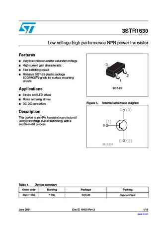
3STR1630 Low voltage high performance NPN power transistor Features Very low collector-emitter saturation voltage 3 High current gain characteristic Fast switching speed Miniature SOT-23 plastic package 2 ECOPACK 2 grade for surface mounting 1 circuits SOT-23 Applications Strobe and LED drives Motor and relay drives Figure 1. Internal schematic diagram... See More ⇒
irf630.pdf
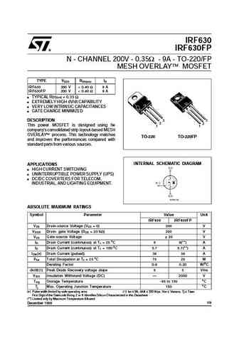
IRF630 IRF630FP N - CHANNEL 200V - 0.35 - 9A - TO-220/FP MESH OVERLAY MOSFET TYPE VDSS RDS(on) ID IRF630 200 V ... See More ⇒
irf630mfp.pdf
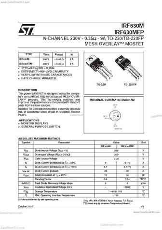
www.DataSheet4U.com IRF630M IRF630MFP N-CHANNEL 200V - 0.35 - 9A TO-220/TO-220FP MESH OVERLAY MOSFET TYPE VDSS RDS(on) ID IRF630M 200 V ... See More ⇒
irf630m.pdf
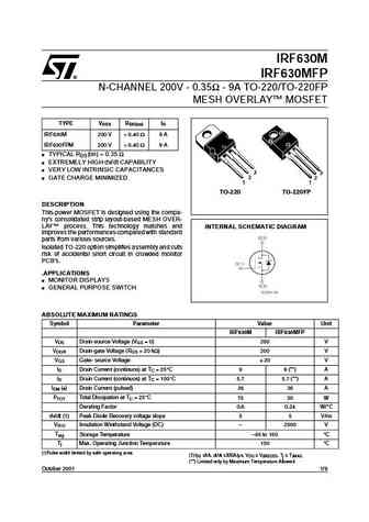
IRF630M IRF630MFP N-CHANNEL 200V - 0.35 - 9A TO-220/TO-220FP MESH OVERLAY MOSFET TYPE VDSS RDS(on) ID IRF630M 200 V ... See More ⇒
irf630s.pdf
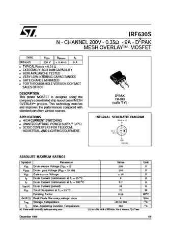
IRF630S N - CHANNEL 200V - 0.35 - 9A- D2PAK MESH OVERLAY MOSFET TYPE VDSS RDS(on) ID IRF630S 200 V ... See More ⇒
irf630 irf630fp.pdf
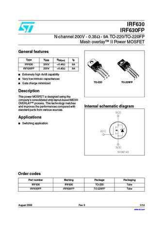
IRF630 IRF630FP N-channel 200V - 0.35 - 9A TO-220/TO-220FP Mesh overlay II Power MOSFET General features Type VDSS RDS(on) ID IRF630 200V ... See More ⇒
mp6301.pdf
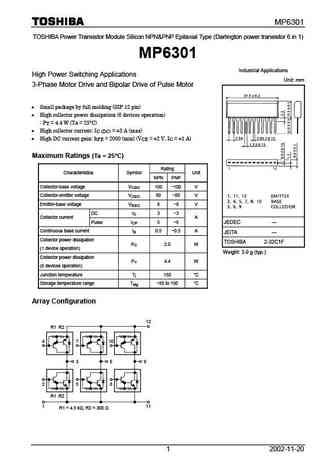
MP6301 TOSHIBA Power Transistor Module Silicon NPN&PNP Epitaxial Type (Darlington power transistor 6 in 1) MP6301 Industrial Applications High Power Switching Applications Unit mm 3-Phase Motor Drive and Bipolar Drive of Pulse Motor Small package by full molding (SIP 12 pin) High collector power dissipation (6 devices operation) P = 4.4 W (Ta = 25 C) T High c... See More ⇒
mp6301 .pdf
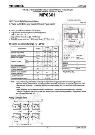
MP6301 TOSHIBA Power Transistor Module Silicon NPN&PNP Epitaxial Type (Six Darlington Power Transistors inOne) MP6301 Industrial Applications High Power Switching Applications Unit mm 3-Phase Motor Drive and Bipolar Drive of Pulse Motor Small package by full molding (SIP 12 pins) High collector power dissipation (6-device operation) PT = 4.4 W (Ta = 25 C) Hi... See More ⇒
2sc4630.pdf
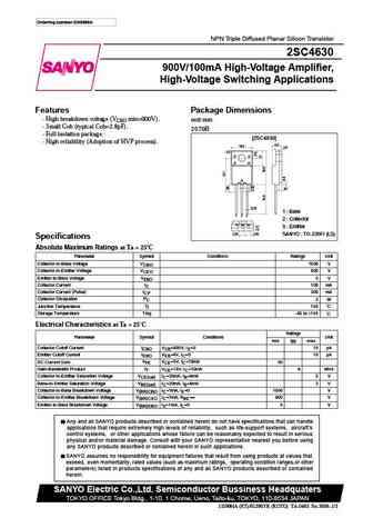
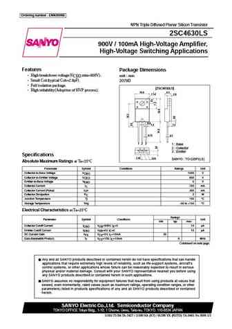
Ordering number EN3699A NPN Triple Diffused Planar Silicon Transistor 2SC4630 900V/100mA High-Voltage Amplifier, High-Voltage Switching Applications Features Package Dimensions High breakdown voltage (VCEO min=900V). unit mm Small Cob (typical Cob=2.8pF). 2079B Full isolation package. [2SC4630] High reliability (Adoption of HVP process). 4.5 10.0 2.8 3.2 0.9 0.... See More ⇒
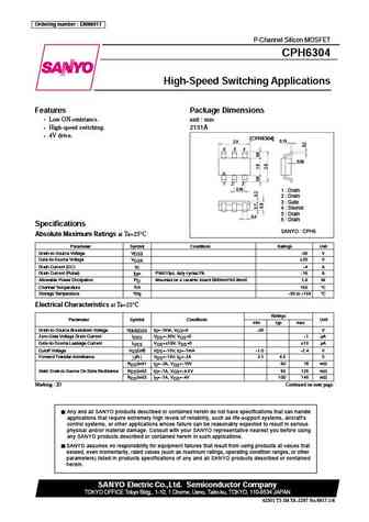
cph6304.pdf
Ordering number ENN6917 CPH6304 P-Channel Silicon MOSFET CPH6304 High-Speed Switching Applications Preliminary Features Package Dimensions Low ON-resistance. unit mm High-speed switching. 2151A 4V drive. [CPH6304] 0.15 2.9 6 5 4 0.05 1 2 3 0.95 1 Drain 2 Drain 3 Gate 4 Source 5 Drain 0.4 6 Drain Specifications SANYO CPH6 Absolute Maximum R... See More ⇒
mch6307.pdf
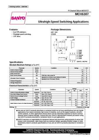
Ordering number ENN7080 MCH6307 P-Channel Silicon MOSFET MCH6307 Ultrahigh-Speed Switching Applications Preliminary Features Package Dimensions Low ON-resistance. unit mm Ultrahigh-speed switching. 2193A 1.8V drive. [MCH6307] 0.3 0.15 4 5 6 3 2 1 0.65 1 Drain 2 Drain 2.0 6 5 4 3 Gate 4 Source 5 Drain 6 Drain 1 2 3 SANYO MCPH6 Specifications ... See More ⇒
cph6302.pdf
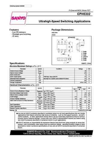
Ordering number EN5939 P-Channel MOS Silicon FET CPH6302 Ultrahigh-Speed Switching Applications Features Package Dimensions Low ON resistance. unit mm Ultrahigh-speed switching. 2151 4V drive. [CPH6302] 0.15 2.9 6 5 4 0 to 0.1 1 Drain 1 2 3 2 Drain 0.95 3 Gate 4 Source 5 Drain 6 Drain 0.4 SANYO CPH6 Specifications Absolute Maximum Ratings at T... See More ⇒
cph6306.pdf
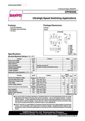
Ordering number ENN6348 P-Channel Silicon MOSFET CPH6306 Ultrahigh-Speed Switching Applications Features Package Dimensions Low ON resistance. unit mm Ultrahigh-speed switching. 2151A 4V drive. [CPH6306] 0.15 2.9 6 5 4 0.05 1 2 3 0.95 1 Drain 2 Drain 3 Gate 4 Source 5 Drain 0.4 6 Drain SANYO CPH6 Specifications Absolute Maximum Ratings at Ta =... See More ⇒
cph6301.pdf
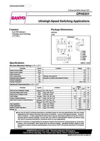
Ordering number EN5938 P-Channel MOS Silicon FET CPH6301 Ultrahigh-Speed Switching Applications Features Package Dimensions Low ON resistance. unit mm Ultrahigh-speed switching. 2151 2.5V drive. [CPH6301] 0.15 2.9 6 5 4 0 to 0.1 1 Drain 1 2 3 2 Drain 0.95 3 Gate 4 Source 5 Drain 6 Drain 0.4 SANYO CPH6 Specifications Absolute Maximum Ratings at... See More ⇒
mch6303.pdf
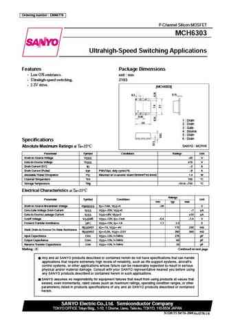
Ordering number ENN6778 MCH6303 P-Channel Silicon MOSFET MCH6303 Ultrahigh-Speed Switching Applications Features Package Dimensions Low ON-resistance. unit mm Ultrahigh-speed switching. 2193 2.5V drive. [MCH6303] 0.3 0.15 6 5 4 1 2 3 0.65 1 Drain 2.0 2 Drain 3 Gate 4 Source 5 Drain 6 Drain Specifications SANYO MCPH6 Absolute Maximum Ratings a... See More ⇒
mch6305.pdf
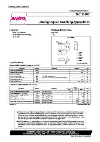
Ordering number ENN6943 MCH6305 P-Channel Silicon MOSFET MCH6305 Ultrahigh-Speed Switching Applications Features Package Dimensions Low ON-resistance. unit mm Ultrahigh-speed switching. 2193 2.5V drive. [MCH6305] 0.3 0.15 6 5 4 1 2 3 0.65 1 Drain 2.0 2 Drain 3 Gate 4 Source 5 Drain 6 Drain Specifications SANYO MCPH6 Absolute Maximum Ratings at... See More ⇒
cph6303.pdf
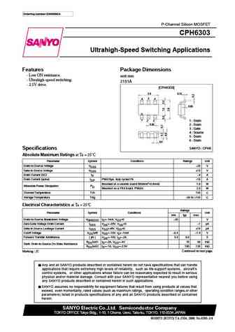
Ordering number ENN6395A P-Channel Silicon MOSFET CPH6303 Ultrahigh-Speed Switching Applications Features Package Dimensions Low ON resistance. unit mm Ultrahigh-speed switching. 2151A 2.5V drive. [CPH6303] 0.15 2.9 6 5 4 0.05 1 2 3 1 Drain 0.95 2 Drain 3 Gate 4 Source 5 Drain 6 Drain 0.4 SANYO CPH6 Specifications Absolute Maximum Ratings at T... See More ⇒
mch6302.pdf
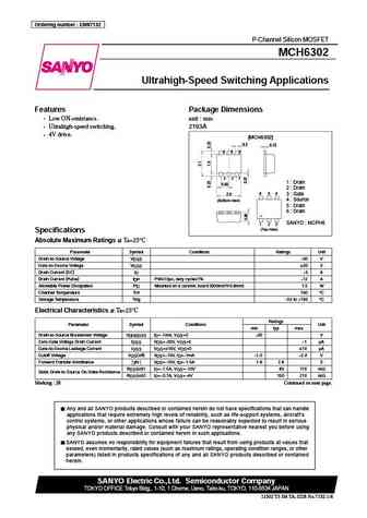
Ordering number ENN7132 MCH6302 P-Channel Silicon MOSFET MCH6302 Ultrahigh-Speed Switching Applications Preliminary Features Package Dimensions Low ON-resistance. unit mm Ultrahigh-speed switching. 2193A 4V drive. [MCH6302] 0.3 0.15 4 5 6 3 2 1 1 Drain 0.65 2 Drain 6 5 4 2.0 3 Gate (Bottom view) 4 Source 5 Drain 6 Drain SANYO MCPH6 1 2 3 (T... See More ⇒
2sc4630ls.pdf
Ordering number ENN3699B 2SC4630LS NPN Triple Diffused Planar Silicon Transistor 2SC4630LS 900V / 100mA High-Voltage Amplifier, High-Voltage Switching Applications Features Package Dimensions High breakdown voltage(VCEO min=900V). unit mm Small Cob(typical Cob=2.8pF). 2079D Full isolation package. [2SC4630LS] High reliability(Adoption of HVP process). 10.0 4.5... See More ⇒
rjk0630jpe.pdf
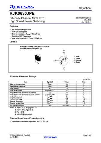
Preliminary Datasheet RJK0630JPE R07DS0340EJ0100 Silicon N Channel MOS FET Rev.1.00 High Speed Power Switching Apr 18, 2011 Features For Automotive application AEC-Q101 compliant Low on-resistance RDS(on) = 6.2 m typ. Capable of 4.5 V gate drive Low input capacitance Ciss = 2100 pF typ. Outline RENESAS Package code PRSS0004AE-B (Package name... See More ⇒
rej03g1630 rjk1021dpeds.pdf
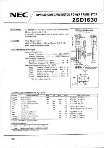
To our customers, Old Company Name in Catalogs and Other Documents On April 1st, 2010, NEC Electronics Corporation merged with Renesas Technology Corporation, and Renesas Electronics Corporation took over all the business of both companies. Therefore, although the old company name remains in this document, it is a valid Renesas Electronics document. We appreciate your understanding. ... See More ⇒
fqpf630.pdf
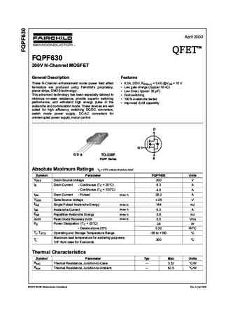
April 2000 TM QFET QFET QFET QFET 200V N-ChanneI MOSFET GeneraI Description Features These N-Channel enhancement mode power field effect 6.3A, 200V, RDS(on) = 0.4 @VGS = 10 V transistors are produced using Fairchild s proprietary, Low gate charge ( typical 19 nC) planar stripe, DMOS technology. Low Crss ( typical 35 pF) This advanced technology has been es... See More ⇒
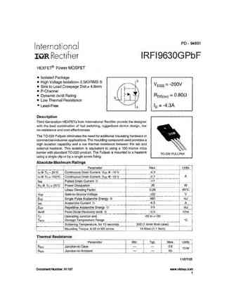
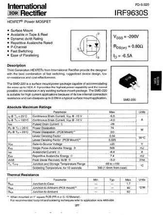
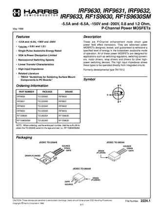
irf9630 rf1s9630sm.pdf
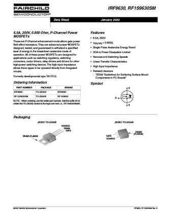
IRF9630, RF1S9630SM Data Sheet January 2002 6.5A, 200V, 0.800 Ohm, P-Channel Power Features MOSFETs 6.5A, 200V These are P-Channel enhancement mode silicon gate power rDS(ON) = 0.800 field effect transistors. They are advanced power MOSFETs Single Pulse Avalanche Energy Rated designed, tested, and guaranteed to withstand a specified level of energy in the breakdown a... See More ⇒
irfw630b irfi630b.pdf
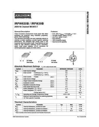
IRFW630B / IRFI630B 200V N-Channel MOSFET General Description Features These N-Channel enhancement mode power field effect 9.0A, 200V, RDS(on) = 0.4 @VGS = 10 V transistors are produced using Fairchild s proprietary, Low gate charge ( typical 22 nC) planar, DMOS technology. Low Crss ( typical 22 pF) This advanced technology has been especially tailored to Fast switc... See More ⇒
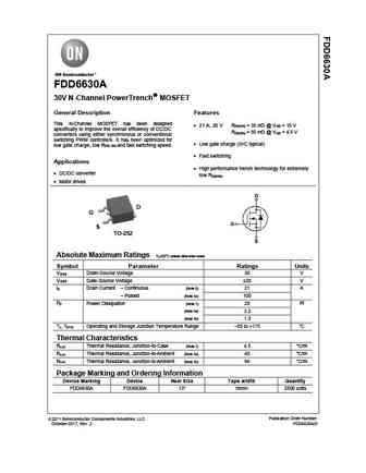
fdd6630a.pdf
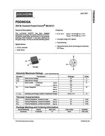
April 2001 FDD6630A 30V N-Channel PowerTrench MOSFET General Description Features This N-Channel MOSFET has been designed 21 A, 30 V R = 35 m @ V = 10 V DS(ON) GS specifically to improve the overall efficiency of DC/DC R = 50 m @ V = 4.5 V DS(ON) GS converters using either synchronous or conventional switching PWM controllers. It has been optimized for Low g... See More ⇒

irf630 rf1s630sm.pdf
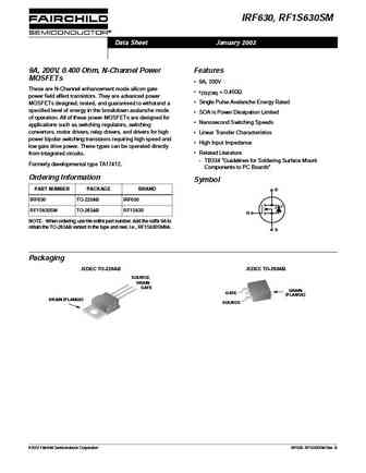
IRF630, RF1S630SM Data Sheet January 2002 9A, 200V, 0.400 Ohm, N-Channel Power Features MOSFETs 9A, 200V These are N-Channel enhancement mode silicon gate rDS(ON) = 0.400 power field effect transistors. They are advanced power Single Pulse Avalanche Energy Rated MOSFETs designed, tested, and guaranteed to withstand a specified level of energy in the breakdown avalanc... See More ⇒
irf630b.pdf
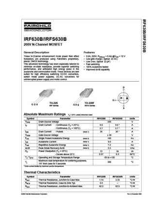
IRF630B/IRFS630B 200V N-Channel MOSFET General Description Features These N-Channel enhancement mode power field effect 9.0A, 200V, RDS(on) = 0.4 @VGS = 10 V transistors are produced using Fairchild s proprietary, Low gate charge ( typical 22 nC) planar, DMOS technology. Low Crss ( typical 22 pF) This advanced technology has been especially tailored to Fast switchin... See More ⇒
fdc6305n.pdf
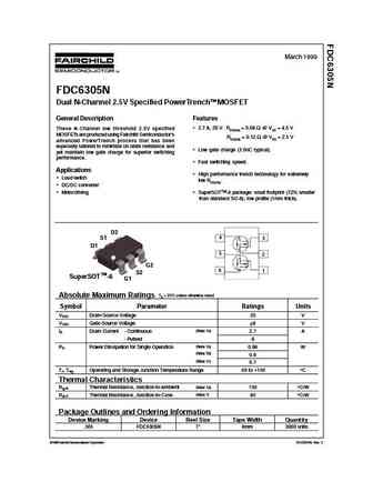
March 1999 FDC6305N Dual N-Channel 2.5V Specified PowerTrenchTM MOSFET General Description Features 2.7 A, 20 V. RDS(ON) = 0.08 @ VGS = 4.5 V These N-Channel low threshold 2.5V specified MOSFETs are produced using Fairchild Semiconductor's RDS(ON) = 0.12 @ VGS = 2.5 V advanced PowerTrench process that has been especially tailored to minimize on-state resistance and Low... See More ⇒
fqp630tstu.pdf
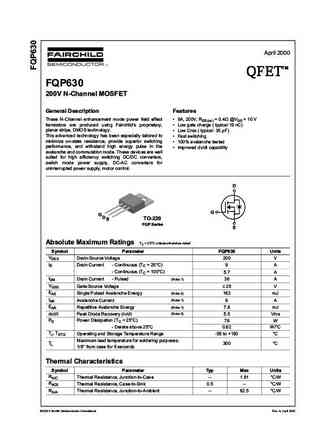
April 2000 TM QFET QFET QFET QFET 200V N-ChanneI MOSFET GeneraI Description Features These N-Channel enhancement mode power field effect 9A, 200V, RDS(on) = 0.4 @VGS = 10 V transistors are produced using Fairchild s proprietary, Low gate charge ( typical 19 nC) planar stripe, DMOS technology. Low Crss ( typical 35 pF) This advanced technology has been espec... See More ⇒
fds6630a.pdf
April 1999 FDS6630A N-Channel Logic Level PowerTrenchTM MOSFET General Description Features This N-Channel Logic Level MOSFET is produced using 6.5 A, 30 V. RDS(on) = 0.038 @ VGS = 10 V Fairchild Semiconductor's advanced PowerTrench process that has been especially tailored to minimize on-state RDS(on) = 0.053 @ VGS = 4.5 V resistance and yet maintain superior switching pe... See More ⇒
fqd630tf fqd630tm.pdf
April 2000 TM QFET QFET QFET QFET 200V N-ChanneI MOSFET GeneraI Description Features These N-Channel enhancement mode power field effect 7A, 200V, RDS(on) = 0.4 @VGS = 10 V transistors are produced using Fairchild s proprietary, Low gate charge ( typical 19 nC) planar stripe, DMOS technology. Low Crss ( typical 35 pF) This advanced technology has b... See More ⇒
sfi9630 sfw9630.pdf
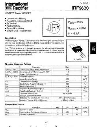
SFW/I9630 Advanced Power MOSFET FEATURES BVDSS = -200 V Avalanche Rugged Technology RDS(on) = 0.8 Rugged Gate Oxide Technology Lower Input Capacitance ID = -6.5 A Improved Gate Charge Extended Safe Operating Area D2-PAK I2-PAK Lower Leakage Current 10 A (Max.) @ VDS = -200V 2 Low RDS(ON) 0.581 (Typ.) 1 1 2 3 3 1. Gate 2. Drain 3. Source Absolute Maximu... See More ⇒
fdg6301n f085.pdf
March 2009 FDG6301N_F085 Dual N-Channel, Digital FET General Description Features 25 V, 0.22 A continuous, 0.65 A peak. These dual N-Channel logic level enhancement mode field effect transistors are produced using Fairchild's RDS(ON) = 4 @ VGS= 4.5 V, proprietary, high cell density, DMOS technology. This RDS(ON) = 5 @ VGS= 2.7 V. very high density process is especially tailor... See More ⇒
fdg6301n.pdf
July 1999 FDG6301N Dual N-Channel, Digital FET General Description Features 25 V, 0.22 A continuous, 0.65 A peak. These dual N-Channel logic level enhancement mode field effect transistors are produced using Fairchild's RDS(ON) = 4 @ VGS= 4.5 V, proprietary, high cell density, DMOS technology. This RDS(ON) = 5 @ VGS= 2.7 V. very high density process is especially tailored to ... See More ⇒
fdg6308p.pdf
October 2000 PRELIMINARY FDG6308P P-Channel 1.8V Specified PowerTrench MOSFET General Description Features This P-Channel 1.8V specified MOSFET uses 0.6 A, 20 V. RDS(ON) = 0.40 @ VGS = 4.5 V Fairchild s advanced low voltage PowerTrench process. RDS(ON) = 0.55 @ VGS = 2.5 V It has been optimized for battery power management RDS(ON) = 0.80 ... See More ⇒
fqb630tm.pdf
April 2000 TM QFET QFET QFET QFET 200V N-ChanneI MOSFET GeneraI Description Features These N-Channel enhancement mode power field effect 9A, 200V, RDS(on) = 0.4 @VGS = 10 V transistors are produced using Fairchild s proprietary, Low gate charge ( typical 19 nC) planar stripe, DMOS technology. Low Crss ( typical 35 pF) This advanced technology has b... See More ⇒
fdc6306p.pdf
February 1999 FDC6306P Dual P-Channel 2.5V Specified PowerTrench MOSFET Features General Description These P-Channel 2.5V specified MOSFETs are produced -1.9 A, -20 V. RDS(on) = 0.170 @ VGS = -4.5 V using Fairchild Semiconductor's advanced PowerTrench RDS(on) = 0.250 @ VGS = -2.5 V process that has been especially tailored to minimize on-state resistance and yet maintain... See More ⇒
fdbl0630n150.pdf
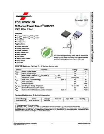
November 2014 FDBL0630N150 N-Channel Power Trench MOSFET 150V, 169A, 6.3m Features Typ rDS(on) = 5m at VGS = 10V, ID = 80A Typ Qg(tot) = 70nC at VGS = 10V, ID = 80A D UIS Capability RoHS Compliant Applications Industrial Motor Drive G Industrial Power Supply Industrial Automation Battery Operated tools S Battery Protection For current package drawing, ple... See More ⇒
fdc6304p.pdf
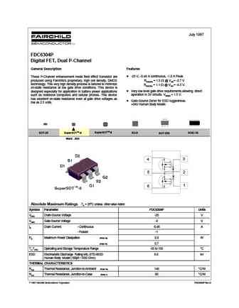
July 1997 FDC6304P Digital FET, Dual P-Channel General Description Features -25 V, -0.46 A continuous, -1.0 A Peak. These P-Channel enhancement mode field effect transistor are produced using Fairchild's proprietary, high cell density, DMOS RDS(ON) = 1.5 @ VGS= -2.7 V technology. This very high density process is tailored to minimize RDS(ON) = 1.1 @ VGS = -4.5 V. on-state ... See More ⇒
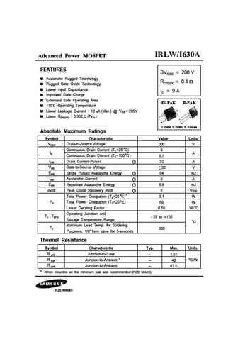
irlw630a irli630a.pdf
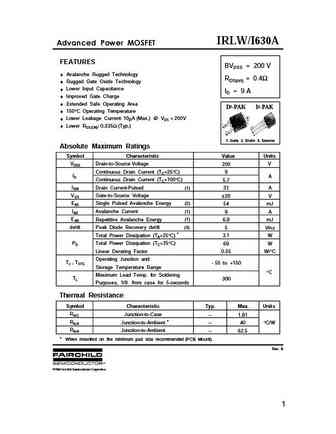
IRLW/I630A FEATURES BVDSS = 200 V Avalanche Rugged Technology RDS(on) = 0.4 Rugged Gate Oxide Technology Lower Input Capacitance ID = 9 A Improved Gate Charge Extended Safe Operating Area D2-PAK I2-PAK 150 C Operating Temperature 2 Lower Leakage Current 10 A (Max.) @ VDS = 200V Lower RDS(ON) 0.335 (Typ.) 1 1 2 3 3 1. Gate 2. Drain 3... See More ⇒
fpn630.pdf
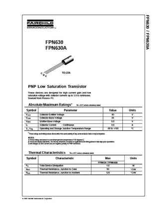
FPN630 FPN630A TO-226 C B E PNP Low Saturation Transistor These devices are designed for high current gain and low saturation voltage with collector currents up to 3.0 A continuous. Sourced from Process PC. Absolute Maximum Ratings* TA = 25 C unless otherwise noted Symbol Parameter Value Units VCEO Collector-Emitter Voltage 30 V VCBO Collector-Base Voltage 35 V VEBO Emitter-Base ... See More ⇒
fdg6306p.pdf
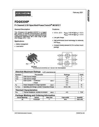
February 2001 FDG6306P P-Channel 2.5V Specified PowerTrench MOSFET General Description Features This P 2.5V specified MOSFET is a rugged -Channel 0.6 A, 20 V. R = 420 m @ V = 4.5 V DS(ON) GS gate version of Fairchild Semiconductor s advanced R = 630 m @ V = 2.5 V DS(ON) GS PowerTrench process. It has been optimized for power management applications... See More ⇒
fdc6302p.pdf
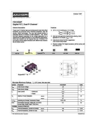
October 1997 FDC6302P Digital FET, Dual P-Channel General Description Features These Dual P-Channel logic level enhancement mode field effect -25 V, -0.12 A continuous, -0.5 A Peak. transistors are produced using Fairchild's proprietary, high cell RDS(ON) = 13 @ VGS= -2.7 V density, DMOS technology. This very high density process is RDS(ON) = 10 @ VGS = -4.5 V. especially... See More ⇒
fdg6303n.pdf
September 2001 FDG6303N Dual N-Channel, Digital FET General Description Features 25 V, 0.50 A continuous, 1.5 A peak. These dual N-Channel logic level enhancement mode RDS(ON) = 0.45 @ VGS= 4.5 V, field effect transistors are produced using Fairchild's proprietary, high cell density, DMOS technology. This RDS(ON) =0.60 @ VGS= 2.7 V. very high density process is especially ta... See More ⇒
irfw630b.pdf
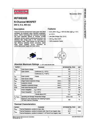
November 2013 IRFW630B N-Channel MOSFET 200 V, 9 A, 400 m Features Description These N-Channel enhancement mode power field effect 9.0 A, 200 V, RDS(on) = 400 m (Max.) @ VGS = 10 V, transistors are produced using Fairchild s proprietary, ID = 4.5 A planar, DMOS technology.This advanced technology has been especially tailored to minimize on-state Low Gate Charge (Typ.... See More ⇒
fdms86300dc.pdf
December 2014 FDMS86300DC N-Channel Dual CoolTM PowerTrench MOSFET 80 V, 110 A, 3.1 m Features General Description Dual CoolTM Top Side Cooling PQFN package This N-Channel MOSFET is produced using Fairchild Semiconductor s advanced PowerTrench process. Max rDS(on) = 3.1 m at VGS = 10 V, ID = 24 A Advancements in both silicon and Dual CoolTM package Max rDS(on) = 4.0 m a... See More ⇒
fdg6304p.pdf
July 1999 FDG6304P Dual P-Channel, Digital FET General Description Features -25 V, -0.41 A continuous, -1.5 A peak. These dual P-Channel logic level enhancement mode RDS(ON) = 1.1 @ VGS= -4.5 V, field effect transistors are produced using Fairchild's proprietary, high cell density, DMOS technology. This RDS(ON) = 1.5 @ VGS= -2.7 V. very high density process is especially ta... See More ⇒
fdc6301n.pdf
September 2001 FDC6301N Dual N-Channel , Digital FET General Description Features 25 V, 0.22 A continuous, 0.5 A Peak. These dual N-Channel logic level enhancement mode field effect transistors are produced using Fairchild 's proprietary, RDS(ON) = 5 @ VGS= 2.7 V high cell density, DMOS technology. This very high density RDS(ON) = 4 @ VGS= 4.5 V. process is especially tailo... See More ⇒
fdg6302p.pdf

July 1999 FDG6302P Dual P-Channel, Digital FET General Description Features -25 V, -0.14 A continuous, -0.4 A peak. These dual P-Channel logic level enhancement mode RDS(ON) = 10 @ VGS= -4.5 V, field effect transistors are produced using Fairchild's proprietary, high cell density, DMOS technology. This RDS(ON) = 13 @ VGS= -2.7 V. very high density process is especially tail... See More ⇒
fdc6308p.pdf
July 1999 FDC6308P Dual P-Channel 2.5V Specified PowerTrenchTM MOSFET General Description Features This P-Channel 2.5V specified MOSFET is a rugged -1.7 A, -18 V. RDS(ON) = 0.18 @ VGS = -4.5 V gate version of Fairchild Semiconductor's advanced RDS(ON) = 0.30 @ VGS = -2.5 V PowerTrench process. It has been optimized for power management applications with a wide range of gate ... See More ⇒
fdc6303n.pdf
August 1997 FDC6303N Digital FET, Dual N-Channel General Description Features 25 V, 0.68 A continuous, 2 A Peak. These dual N-Channel logic level enhancement mode field RDS(ON) = 0.6 @ VGS = 2.7 V effect transistors are produced using Fairchild's proprietary, high cell density, DMOS technology. This very high density RDS(ON) = 0.45 @ VGS= 4.5 V. process is especially tailored... See More ⇒
fdma7630.pdf
September 2010 FDMA7630 Single N-Channel PowerTrench MOSFET 30 V, 11 A, 13 m Features General Description Max rDS(on) = 13 m at VGS = 10 V, ID = 11 A This device has been designed to provide maximum efficiency and thermal performance for synchronous buck converters. The Max rDS(on) = 20 m at VGS = 4.5 V, ID = 9 A low rDS(on) and gate charge provide excellent switching ... See More ⇒
fdms86300.pdf
August 2011 FDMS86300 N-Channel PowerTrench MOSFET 80 V, 42 A, 3.9 m Features General Description Max rDS(on) = 3.9 m at VGS = 10 V, ID = 19 A This N-Channel MOSFET has been designed specifically to improve the overall efficiency and to minimize switch node Max rDS(on) = 5.5 m at VGS = 8 V, ID = 15.5 A ringing of DC/DC converters using either synchronous or Advanced Pac... See More ⇒
fqp630.pdf

April 2000 TM QFET QFET QFET QFET 200V N-ChanneI MOSFET GeneraI Description Features These N-Channel enhancement mode power field effect 9A, 200V, RDS(on) = 0.4 @VGS = 10 V transistors are produced using Fairchild s proprietary, Low gate charge ( typical 19 nC) planar stripe, DMOS technology. Low Crss ( typical 35 pF) This advanced technology has been espec... See More ⇒
fdn5630.pdf
March 2000 FDN5630 60V N-Channel PowerTrench MOSFET General Description Features This N-Channel MOSFET has been designed specifically 1.7 A, 60 V. RDS(ON) = 0.100 @ VGS = 10 V to improve the overall efficiency of DC/DC converters using RDS(ON) = 0.120 @ VGS = 6 V. either synchronous or conventional switching PWM Optimized for use in high frequenc... See More ⇒
pbss5630pa.pdf

Important notice Dear Customer, On 7 February 2017 the former NXP Standard Product business became a new company with the tradename Nexperia. Nexperia is an industry leading supplier of Discrete, Logic and PowerMOS semiconductors with its focus on the automotive, industrial, computing, consumer and wearable application markets In data sheets and application notes which still contain... See More ⇒
pbss4630pa.pdf

Important notice Dear Customer, On 7 February 2017 the former NXP Standard Product business became a new company with the tradename Nexperia. Nexperia is an industry leading supplier of Discrete, Logic and PowerMOS semiconductors with its focus on the automotive, industrial, computing, consumer and wearable application markets In data sheets and application notes which still contain... See More ⇒
irfw630a.pdf
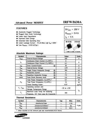
Advanced Power MOSFET FEATURES BVDSS = 200 V Avalanche Rugged Technology RDS(on) = 0.4 Rugged Gate Oxide Technology Lower Input Capacitance ID = 9 A Improved Gate Charge Extended Safe Operating Area Lower Leakage Current 10 A (Max.) @ VDS = 200V 2 Low RDS(ON) 0.333 (Typ.) 1 1 2 3 3 1. Gate 2. Drain 3. Source Absolute Maximum Ratings Symbol Charact... See More ⇒
sfs9630.pdf
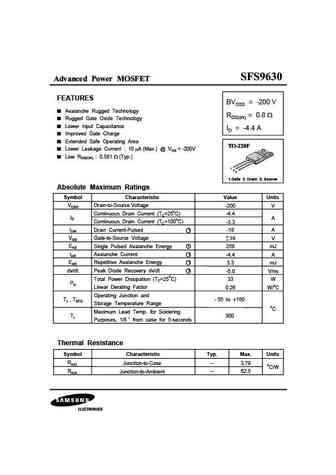
Advanced Power MOSFET FEATURES BVDSS = -200 V Avalanche Rugged Technology RDS(on) = 0.8 Rugged Gate Oxide Technology Lower Input Capacitance ID = -4.4 A Improved Gate Charge Extended Safe Operating Area Lower Leakage Current 10 A (Max.) @ VDS = -200V Low RDS(ON) 0.581 (Typ.) 1 2 3 1.Gate 2. Drain 3. Source Absolute Maximum Ratings Symbol Characteristic V... See More ⇒
irfs630a.pdf
Advanced Power MOSFET FEATURES BVDSS = 200 V Avalanche Rugged Technology RDS(on) = 0.4 Rugged Gate Oxide Technology Lower Input Capacitance ID = 6.5 A Improved Gate Charge Extended Safe Operating Area Lower Leakage Current 10 A (Max.) @ VDS = 200V Low RDS(ON) 0.333 (Typ.) 1 2 3 1.Gate 2. Drain 3. Source Absolute Maximum Ratings Symbol Characteristic Valu... See More ⇒
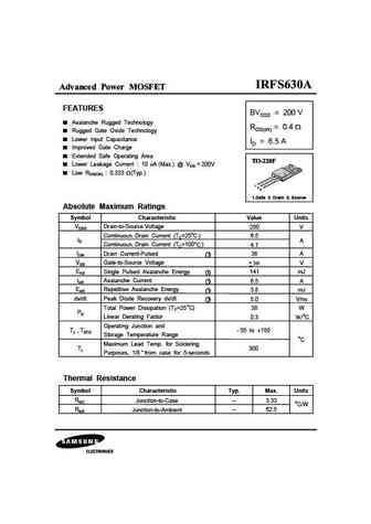
irl630a.pdf
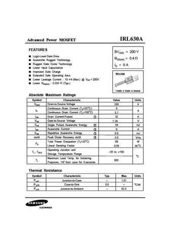
Advanced Power MOSFET FEATURES BVDSS = 200 V Logic-Level Gate Drive RDS(on) = 0.4 Avalanche Rugged Technology Rugged Gate Oxide Technology ID = 9 A Lower Input Capacitance Improved Gate Charge Extended Safe Operating Area Lower Leakage Current 10 A (Max.) @ VDS = 200V Lower RDS(ON) 0.335 (Typ.) 1 2 3 1.Gate 2. Drain 3. Source Absolute Maximum Ratings... See More ⇒
irf9230 irf9231 irf9232 irf9233 irfp9230 irfp9231 irfp9232 irfp9233 irf9630 irf9631 irf9632 irf9633.pdf
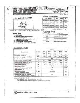
... See More ⇒
irf630a.pdf
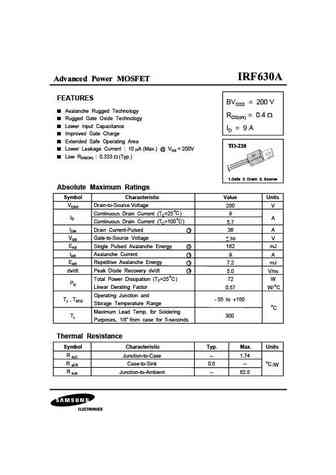
Advanced Power MOSFET FEATURES BVDSS = 200 V Avalanche Rugged Technology RDS(on) = 0.4 Rugged Gate Oxide Technology Lower Input Capacitance ID = 9 A Improved Gate Charge Extended Safe Operating Area Lower Leakage Current 10 A (Max.) @ VDS = 200V Low RDS(ON) 0.333 (Typ.) 1 2 3 1.Gate 2. Drain 3. Source Absolute Maximum Ratings Symbol Characteristic Value ... See More ⇒
irls630a.pdf
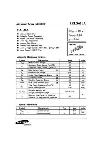
Advanced Power MOSFET FEATURES BVDSS = 200 V Logic Level Gate Drive RDS(on) = 0.4 Avalanche Rugged Technology Rugged Gate Oxide Technology ID = 6.5 A Lower Input Capacitance Improved Gate Charge Extended Safe Operating Area Lower Leakage Current 10 A (Max.) @ VDS = 200V Lower RDS(ON) 0.335 (Typ.) 1 2 3 1.Gate 2. Drain 3. Source Absolute Maximum Ratin... See More ⇒
irlw630a.pdf
Advanced Power MOSFET FEATURES BVDSS = 200 V Avalanche Rugged Technology RDS(on) = 0.4 Rugged Gate Oxide Technology Lower Input Capacitance ID = 9 A Improved Gate Charge Extended Safe Operating Area 175 Operating Temperature 2 Lower Leakage Current 10 A (Max.) @ VDS = 200V Lower RDS(ON) 0.335 (Typ.) 1 1 2 3 3 1. Gate 2. Drain 3. Source Absolute M... See More ⇒
sfp9630.pdf
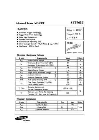
Advanced Power MOSFET FEATURES BVDSS = -200 V Avalanche Rugged Technology RDS(on) = 0.8 Rugged Gate Oxide Technology Lower Input Capacitance ID = -6.5 A Improved Gate Charge Extended Safe Operating Area Lower Leakage Current -10 A (Max.) @ VDS = -200V Low RDS(ON) 0.581 (Typ.) 1 2 3 1.Gate 2. Drain 3. Source Absolute Maximum Ratings Symbol Characteristic ... See More ⇒
sfw9630.pdf
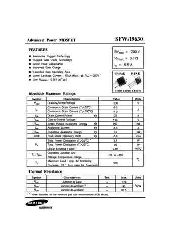
Advanced Power MOSFET FEATURES BVDSS = -200 V Avalanche Rugged Technology RDS(on) = 0.8 Rugged Gate Oxide Technology Lower Input Capacitance ID = -6.5 A Improved Gate Charge Extended Safe Operating Area Lower Leakage Current 10 A (Max.) @ VDS = -200V 2 Low RDS(ON) 0.581 (Typ.) 1 1 2 3 3 1. Gate 2. Drain 3. Source Absolute Maximum Ratings Symbol Ch... See More ⇒
bts630.pdf
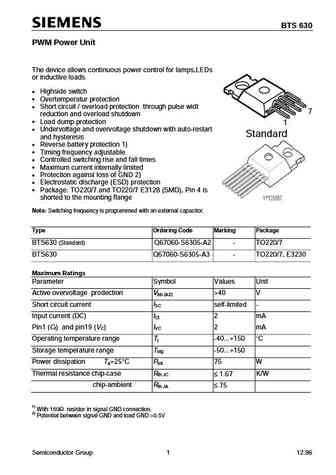
BTS 630 PWM Power Unit The device allows continuous power control for lamps,LEDs or inductive loads. Highside switch Overtemperatur protection Short circuit / overload protection through pulse widt 7 reduction and overload shutdown Load dump protection 1 Undervoltage and overvoltage shutdown with auto-restart Standard and hysteresis Reverse battery protecti... See More ⇒
irf9630pbf sihf9630.pdf
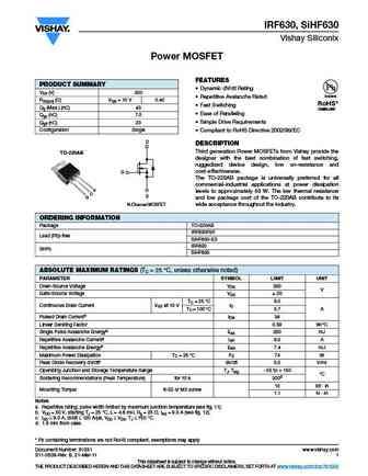
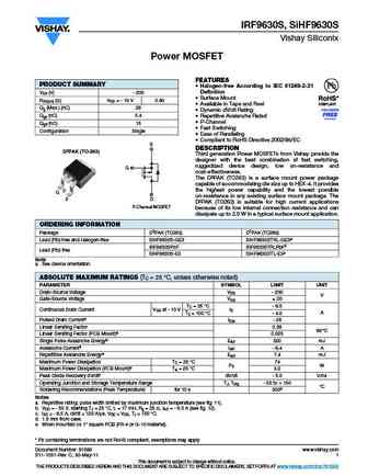
IRF9630, SiHF9630 Vishay Siliconix Power MOSFET FEATURES PRODUCT SUMMARY Dynamic dV/dt Rating VDS (V) - 200 Available Repetitive Avalanche Rated RDS(on) (Max.) ( )VGS = - 10 V 0.80 RoHS* P-Channel Qg (Max.) (nC) 29 COMPLIANT Fast Switching Qgs (nC) 5.4 Ease of Paralleling Qgd (nC) 15 Simple Drive Requirements Configuration Single Compliant to RoH... See More ⇒
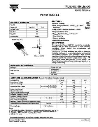
irl630 sihl630.pdf
IRL630, SiHL630 Vishay Siliconix Power MOSFET FEATURES PRODUCT SUMMARY Dynamic dV/dt Rating VDS (V) 200 V Available Repetitive Avalanche Rated RDS(on) ( )VGS = 5 V 0.40 RoHS* Logic Level Gate Drive COMPLIANT Qg (Max.) (nC) 40 RDS(on) Specified at VGS = 4 V and 5 V Qgs (nC) 5.5 150 C Operating Temperature Qgd (nC) 24 Fast Switching Configuration Sing... See More ⇒
irl630s sihl630s.pdf
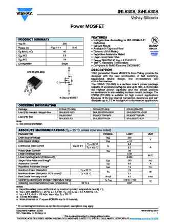
IRL630S, SiHL630S Vishay Siliconix Power MOSFET FEATURES PRODUCT SUMMARY Halogen-free According to IEC 61249-2-21 Definition VDS (V) 200 Surface Mount RDS(on) ( )VGS = 5 V 0.40 Available in Tape and Reel Qg (Max.) (nC) 40 Dynamic dV/dt Rating Repetitive Avalanche Rated Qgs (nC) 5.5 Logic-Level Gate Drive Qgd (nC) 24 RDS(on) Specified at VGS = 4 V a... See More ⇒
irf630spbf sihf630s.pdf
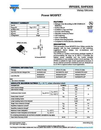
IRF630S, SiHF630S Vishay Siliconix Power MOSFET FEATURES PRODUCT SUMMARY Halogen-free According to IEC 61249-2-21 VDS (V) 200 Definition RDS(on) ( )VGS = 10 V 0.40 Surface Mount Qg (Max.) (nC) 43 Available in Tape and Reel Qgs (nC) 7.0 Dynamic dV/dt Rating Qgd (nC) 23 Repetitive Avalanche Rated Configuration Single Fast Switching Ease of Paralleli... See More ⇒
irl630spbf sihl630s.pdf

IRL630S, SiHL630S Vishay Siliconix Power MOSFET FEATURES PRODUCT SUMMARY Halogen-free According to IEC 61249-2-21 Definition VDS (V) 200 Surface Mount RDS(on) ( )VGS = 5 V 0.40 Available in Tape and Reel Qg (Max.) (nC) 40 Dynamic dV/dt Rating Repetitive Avalanche Rated Qgs (nC) 5.5 Logic-Level Gate Drive Qgd (nC) 24 RDS(on) Specified at VGS = 4 V a... See More ⇒
irfi630g sihfi630g.pdf
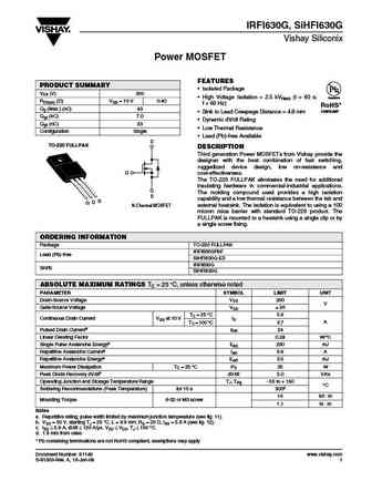
IRFI630G, SiHFI630G Vishay Siliconix Power MOSFET FEATURES PRODUCT SUMMARY Isolated Package VDS (V) 200 High Voltage Isolation = 2.5 kVRMS (t = 60 s; Available RDS(on) ( )VGS = 10 V 0.40 f = 60 Hz) RoHS* Qg (Max.) (nC) 43 COMPLIANT Sink to Lead Creepage Distance = 4.8 mm Qgs (nC) 7.0 Dynamic dV/dt Rating Qgd (nC) 23 Low Thermal Resistance Configuration S... See More ⇒
irfi9630gpbf sihfi9630g.pdf
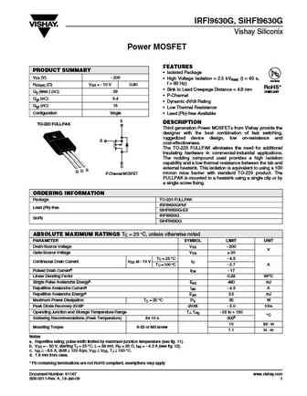
IRFI9630G, SiHFI9630G Vishay Siliconix Power MOSFET FEATURES PRODUCT SUMMARY Isolated Package VDS (V) - 200 High Voltage Isolation = 2.5 kVRMS (t = 60 s, Available f = 60 Hz) RDS(on) ( )VGS = - 10 V 0.80 RoHS* Sink to Lead Creepage Distance = 4.8 mm Qg (Max.) (nC) 29 COMPLIANT P-Channel Qgs (nC) 5.4 Dynamic dV/dt Rating Qgd (nC) 15 Low Thermal Resist... See More ⇒
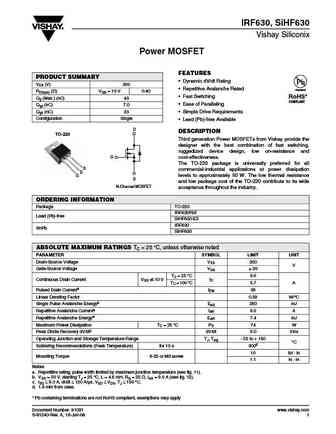
irf630pbf sihf630.pdf
IRF630, SiHF630 Vishay Siliconix Power MOSFET FEATURES PRODUCT SUMMARY Dynamic dV/dt Rating VDS (V) 200 Available Repetitive Avalanche Rated RDS(on) ( )VGS = 10 V 0.40 RoHS* Fast Switching Qg (Max.) (nC) 43 COMPLIANT Ease of Paralleling Qgs (nC) 7.0 Qgd (nC) 23 Simple Drive Requirements Configuration Single Compliant to RoHS Directive 2002/95/EC D D... See More ⇒
irl630pbf sihl630.pdf

IRL630, SiHL630 Vishay Siliconix Power MOSFET FEATURES PRODUCT SUMMARY Dynamic dV/dt Rating VDS (V) 200 V Available Repetitive Avalanche Rated RDS(on) ( )VGS = 5 V 0.40 RoHS* Logic Level Gate Drive COMPLIANT Qg (Max.) (nC) 40 RDS(on) Specified at VGS = 4 V and 5 V Qgs (nC) 5.5 150 C Operating Temperature Qgd (nC) 24 Fast Switching Configuration Sing... See More ⇒
irf9630 sihf9630.pdf

IRF9630, SiHF9630 Vishay Siliconix Power MOSFET FEATURES PRODUCT SUMMARY Dynamic dV/dt Rating VDS (V) - 200 Available Repetitive Avalanche Rated RDS(on) (Max.) ( )VGS = - 10 V 0.80 RoHS* P-Channel Qg (Max.) (nC) 29 COMPLIANT Fast Switching Qgs (nC) 5.4 Ease of Paralleling Qgd (nC) 15 Simple Drive Requirements Configuration Single Compliant to RoH... See More ⇒
si4630dy.pdf
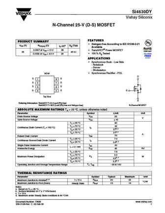
Si4630DY Vishay Siliconix N-Channel 25-V (D-S) MOSFET FEATURES PRODUCT SUMMARY Halogen-free According to IEC 61249-2-21 VDS (V) RDS(on) ( ) ID (A)a Qg (Typ) Available 0.0027 at VGS = 10 V 36 TrenchFET Power MOSFET 25 49 nC 100 % Rg Tested 0.0032 at VGS = 4.5 V 29 APPLICATIONS Synchronous Buck - Low Side - Notebook - Server - Workstation Synchrono... See More ⇒
irf630 sihf630.pdf
IRF630, SiHF630 Vishay Siliconix Power MOSFET FEATURES PRODUCT SUMMARY Dynamic dV/dt Rating VDS (V) 200 Repetitive Avalanche Rated Available RDS(on) ( )VGS = 10 V 0.40 Fast Switching RoHS* Qg (Max.) (nC) 43 COMPLIANT Ease of Paralleling Qgs (nC) 7.0 Qgd (nC) 23 Simple Drive Requirements Configuration Single Lead (Pb)-free Available D DESCRIPTION TO-... See More ⇒
irf9630spbf sihf9630s.pdf

IRF9630S, SiHF9630S Vishay Siliconix Power MOSFET FEATURES PRODUCT SUMMARY Halogen-free According to IEC 61249-2-21 Definition VDS (V) - 200 Surface Mount RDS(on) ( )VGS = - 10 V 0.80 Available in Tape and Reel Qg (Max.) (nC) 29 Dynamic dV/dt Rating Qgs (nC) 5.4 Repetitive Avalanche Rated P-Channel Qgd (nC) 15 Fast Switching Configuration Single ... See More ⇒
irfi9630g sihfi9630g.pdf

IRFI9630G, SiHFI9630G Vishay Siliconix Power MOSFET FEATURES PRODUCT SUMMARY Isolated Package VDS (V) - 200 High Voltage Isolation = 2.5 kVRMS (t = 60 s, Available f = 60 Hz) RDS(on) ( )VGS = - 10 V 0.80 RoHS* Sink to Lead Creepage Distance = 4.8 mm Qg (Max.) (nC) 29 COMPLIANT P-Channel Qgs (nC) 5.4 Dynamic dV/dt Rating Qgd (nC) 15 Low Thermal Resist... See More ⇒
sihli630g.pdf
IRLI630G, SiHLI630G Vishay Siliconix Power MOSFET FEATURES PRODUCT SUMMARY Isolated Package VDS (V) 200 Available High Voltage Isolation = 2.5 kVRMS (t = 60 s; RDS(on) ( )VGS = 5.0 V 0.40 f = 60 Hz) RoHS* COMPLIANT Qg (Max.) (nC) 40 Sink to Lead Creepage Distance = 4.8 mm Qgs (nC) 5.5 Logic-Level Gate Drive Qgd (nC) 24 RDS(on) Specified at VGS = 4 V and 5V ... See More ⇒
sihfi630g.pdf

IRFI630G, SiHFI630G Vishay Siliconix Power MOSFET FEATURES PRODUCT SUMMARY Isolated Package VDS (V) 200 High Voltage Isolation = 2.5 kVRMS (t = 60 s; Available RDS(on) ( )VGS = 10 V 0.40 f = 60 Hz) RoHS* Qg (Max.) (nC) 43 COMPLIANT Sink to Lead Creepage Distance = 4.8 mm Qgs (nC) 7.0 Dynamic dV/dt Rating Qgd (nC) 23 Low Thermal Resistance Configuration S... See More ⇒
irf9630s sihf9630s.pdf
IRF9630S, SiHF9630S Vishay Siliconix Power MOSFET FEATURES PRODUCT SUMMARY Halogen-free According to IEC 61249-2-21 Definition VDS (V) - 200 Surface Mount RDS(on) ( )VGS = - 10 V 0.80 Available in Tape and Reel Qg (Max.) (nC) 29 Dynamic dV/dt Rating Qgs (nC) 5.4 Repetitive Avalanche Rated P-Channel Qgd (nC) 15 Fast Switching Configuration Single ... See More ⇒
irf630s sihf630s.pdf

IRF630S, SiHF630S Vishay Siliconix Power MOSFET FEATURES PRODUCT SUMMARY Halogen-free According to IEC 61249-2-21 VDS (V) 200 Definition RDS(on) ( )VGS = 10 V 0.40 Surface Mount Qg (Max.) (nC) 43 Available in Tape and Reel Qgs (nC) 7.0 Dynamic dV/dt Rating Qgd (nC) 23 Repetitive Avalanche Rated Configuration Single Fast Switching Ease of Paralleli... See More ⇒
2n6306 2n6307 2n6308.pdf
145 Adams Avenue, Hauppauge, NY 11788 USA Tel (631) 435-1110 Fax (631) 435-1824 ... See More ⇒
2n5629 2n5630 2n6029 2n6030.pdf
145 Adams Avenue, Hauppauge, NY 11788 USA Tel (631) 435-1110 Fax (631) 435-1824 ... See More ⇒
dmg6301udw.pdf
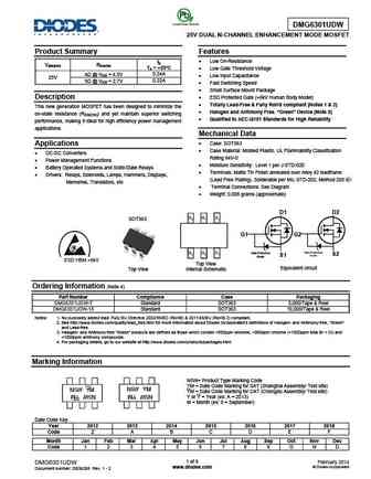
DMG6301UDW 25V DUAL N-CHANNEL ENHANCEMENT MODE MOSFET Product Summary Features Low On-Resistance ID V(BR)DSS RDS(ON) TA = +25 C Low Gate Threshold Voltage 4 @ VGS = 4.5V 0.24A Low Input Capacitance 25V 5 @ VGS = 2.7V 0.22A Fast Switching Speed Small Surface Mount Package Description ESD Protected Gate (>6kV Human Body Model) Totally... See More ⇒
irgb4630dpbf irgib4630dpbf irgp4630dpbf irgs4630dpbf.pdf
IR IGBT IRGB4630DPbF IRGIB4630DPbF IRGP4630D(-E)PbF IRGS4630DPbF Insulated Gate Bipolar Transistor with Ultrafast Soft Recovery Diode VCES = 600V C C C IC = 30A, TC =100 C tSC 5 s, TJ(max) = 175 C E C E E G C G C G VCE(ON) typ. = 1.65V @ IC = 18A IRGP4630DPbF IRGP4630D-EPbF IRGB4630DPbF TO-247AC TO-247AD TO-220AB C C Applications Indust... See More ⇒
6ms16017e33w32630.pdf
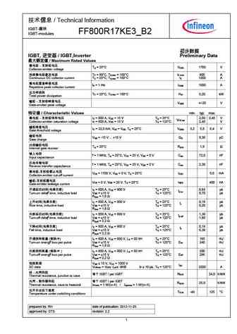
/ Technical Information IGBT- FF800R17KE3_B2 IGBT-modules IGBT, / IGBT,Inverter Preliminary Data / Maximum Rated Values T = 25 C V 1700 V vj CES Collector-emitter voltage T = 80 C, T = 150 C I 800 A C vj max C nom Continuous DC collector current T = 25 C, T = 150 C... See More ⇒
nimd6302r2.pdf
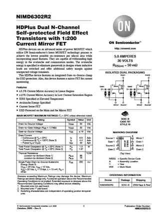
NIMD6302R2 HDPlus Dual N-Channel Self-protected Field Effect Transistors with 1 200 Current Mirror FET http //onsemi.com HDPlus devices are an advanced series of power MOSFET which utilize ON Semiconductor s latest MOSFET technology process to achieve the lowest possible on-resistance per silicon area while 5.0 AMPERES incorporating smart features. They are capable of withstanding h... See More ⇒
fdd6630a.pdf
FDD6630A 30V N-Channel PowerTrench MOSFET General Description Features This N-Channel MOSFET has been designed 21 A, 30 V R = 35 m @ V = 10 V DS(ON) GS specifically to improve the overall efficiency of DC/DC R = 50 m @ V = 4.5 V DS(ON) GS converters using either synchronous or conventional switching PWM controllers. It has been optimized for Low gate charge (5n... See More ⇒
fdc6305n.pdf

Is Now Part of To learn more about ON Semiconductor, please visit our website at www.onsemi.com Please note As part of the Fairchild Semiconductor integration, some of the Fairchild orderable part numbers will need to change in order to meet ON Semiconductor s system requirements. Since the ON Semiconductor product management systems do not have the ability to manage part nomenclatur... See More ⇒
fdb0630n1507l.pdf

Is Now Part of To learn more about ON Semiconductor, please visit our website at www.onsemi.com Please note As part of the Fairchild Semiconductor integration, some of the Fairchild orderable part numbers will need to change in order to meet ON Semiconductor s system requirements. Since the ON Semiconductor product management systems do not have the ability to manage part nomenclatur... See More ⇒
fdg6301n.pdf
Digital FET, Dual N-Channel FDG6301N General Description These dual N-Channel logic level enhancement mode field effect transistors are produced using ON Semiconductor s proprietary, high cell density, DMOS technology. This very high density process is www.onsemi.com especially tailored to minimize on-state resistance. This device has been designed especially for low voltage applicati... See More ⇒
fdc6306p.pdf

Is Now Part of To learn more about ON Semiconductor, please visit our website at www.onsemi.com Please note As part of the Fairchild Semiconductor integration, some of the Fairchild orderable part numbers will need to change in order to meet ON Semiconductor s system requirements. Since the ON Semiconductor product management systems do not have the ability to manage part nomenclatur... See More ⇒
efc4630r.pdf
Ordering number ENA2320 EFC4630R Advance Information http //onsemi.com N-Channel Power MOSFET 24V, 6A, 45m , Dual EFCP Features 2.5V drive Common-drain type Built-in gate protection resistor Halogen free compliance Best suited for LiB charging and discharging switch Specifications Absolute Maximum Ratings at Ta=25 C Parameter Symbol Conditions Value ... See More ⇒
fdg6303n.pdf
FDG6303N Dual N-Channel, Digital FET General Description Features 25 V, 0.50 A continuous, 1.5 A peak. These dual N-Channel logic level enhancement mode RDS(ON) = 0.45 @ VGS= 4.5 V, field effect transistors are produced using ON Semiconductor's proprietary, high cell density, DMOS RDS(ON) =0.60 @ VGS= 2.7 V. technology. This very high density process is Very low level gate... See More ⇒
fdms86300dc.pdf
FDMS86300DC POWERTRENCH) MOSFET, N-Channel, DUAL COOL) 56 80 V, 110 A, 3.1 mW General Description www.onsemi.com This N-Channel MOSFET is produced using Fairchild Semiconductor s advanced POWERTRENCH process that ELECTRICAL CONNECTION incorporates Shielded Gate technology. Advancements in both silicon and DUAL COOL package technologies have been combined to S D offer the lowes... See More ⇒
fdc6301n.pdf
FDC6301N Dual N-Channel , Digital FET Features General Description 25 V, 0.22 A continuous, 0.5 A Peak. These dual N-Channel logic level enhancement mode field RDS(ON) = 5 @ VGS= 2.7 V effect transistors are produced using ON Semiconductor 's RDS(ON) = 4 @ VGS= 4.5 V. proprietary, high cell density, DMOS technology. This very high density process is especially tailored to... See More ⇒
ntmfs5h630nl.pdf
MOSFET Power, Single, N-Channel 60 V, 3.1 mW, 120 A NTMFS5H630NL Features Small Footprint (5x6 mm) for Compact Design www.onsemi.com Low RDS(on) to Minimize Conduction Losses Low QG and Capacitance to Minimize Driver Losses These Devices are Pb-Free and are RoHS Compliant V(BR)DSS RDS(ON) MAX ID MAX 3.1 mW @ 10 V MAXIMUM RATINGS (TJ = 25 C unless otherwise noted... See More ⇒
fdms86300.pdf

Is Now Part of To learn more about ON Semiconductor, please visit our website at www.onsemi.com Please note As part of the Fairchild Semiconductor integration, some of the Fairchild orderable part numbers will need to change in order to meet ON Semiconductor s system requirements. Since the ON Semiconductor product management systems do not have the ability to manage part nomenclatur... See More ⇒
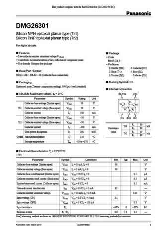
dmg96303.pdf
This product complies with the RoHS Directive (EU 2002/95/EC). DMG96303 Silicon NPN epitaxial planar type (Tr1) Silicon PNP epitaxial planar type (Tr2) For digital circuits Features Package Low collector-emitter saturation voltage VCE(sat) Code Contributes to miniaturization of sets, reduction of component count. SSMini5-F4-B Eco-friendly Halogen-free package ... See More ⇒
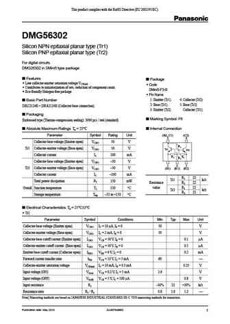
dmg56301.pdf
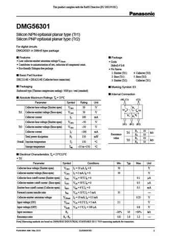
This product complies with the RoHS Directive (EU 2002/95/EC). DMG56301 Silicon NPN epitaxial planar type (Tr1) Silicon PNP epitaxial planar type (Tr2) For digital circuits DMG26301 in SMini5 type package Features Package Low collector-emitter saturation voltage VCE(sat) Code Contributes to miniaturization of sets, reduction of component count. SMini5-F3-B Ec... See More ⇒
dmg96301.pdf
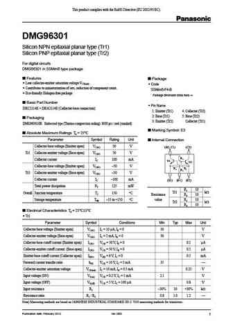
This product complies with the RoHS Directive (EU 2002/95/EC). DMG96301 Silicon NPN epitaxial planar type (Tr1) Silicon PNP epitaxial planar type (Tr2) For digital circuits DMG56301 in SSMini5 type package Features Package Low collector-emitter saturation voltage VCE(sat) Code Contributes to miniaturization of sets, reduction of component count. SSMini5-F4-B ... See More ⇒
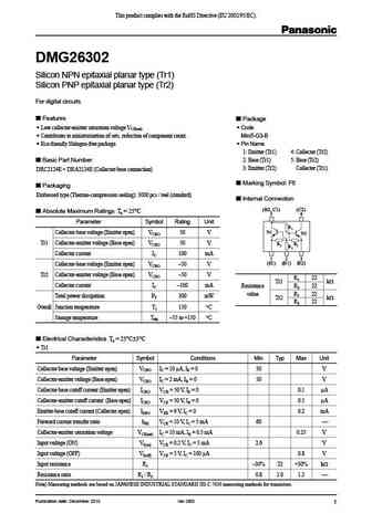
dmg96302.pdf

This product complies with the RoHS Directive (EU 2002/95/EC). DMG96302 Silicon NPN epitaxial planar type (Tr1) Silicon PNP epitaxial planar type (Tr2) For digital circuits DMG56302 in SSMini5 type package Features Package Low collector-emitter saturation voltage VCE(sat) Code Contributes to miniaturization of sets, reduction of component count. SSMini5-F4-B ... See More ⇒
dmg56302.pdf
This product complies with the RoHS Directive (EU 2002/95/EC). DMG56302 Silicon NPN epitaxial planar type (Tr1) Silicon PNP epitaxial planar type (Tr2) For digital circuits DMG26302 in SMini5 type package Features Package Low collector-emitter saturation voltage VCE(sat) Code Contributes to miniaturization of sets, reduction of component count. SMini5-F3-B E... See More ⇒
dmg26302.pdf
This product complies with the RoHS Directive (EU 2002/95/EC). DMG26302 Silicon NPN epitaxial planar type (Tr1) Silicon PNP epitaxial planar type (Tr2) For digital circuits Features Package Low collector-emitter saturation voltage VCE(sat) Code Contributes to miniaturization of sets, reduction of component count. Mini5-G3-B Eco-friendly Halogen-free package ... See More ⇒
dmg56306.pdf
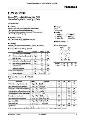
This product complies with the RoHS Directive (EU 2002/95/EC). DMG56306 Silicon NPN epitaxial planar type (Tr1) Silicon PNP epitaxial planar type (Tr2) For digital circuits Features Package High forward current transfer ratio hFE with excellent linearity Code Low collector-emitter saturation voltage VCE(sat) SMini5-F3-B Contributes to miniaturization of sets, ... See More ⇒
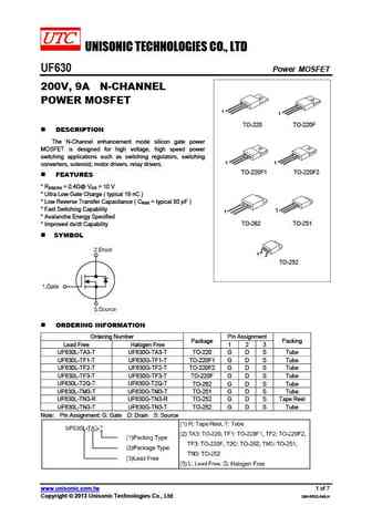
uf630l-tm3-t uf630g-tm3-t uf630l-tn3-r uf630g-tn3-r uf630l-t2q-t uf630g-t2q-t uf630g-s08-r.pdf

UNISONIC TECHNOLOGIES CO., LTD UF630 Power MOSFET 200V, 9A N-CHANNEL POWER MOSFET 1 1 TO-220 TO-220F DESCRIPTION The N-Channel enhancement mode silicon gate power MOSFET is designed for high voltage, high speed power 1 1 switching applications such as switching regulators, switching converters, solenoid, motor drivers, relay drivers. TO-220F1 TO-220F2 FEATURES ... See More ⇒
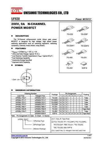
uf630.pdf
UNISONIC TECHNOLOGIES CO., LTD UF630 Power MOSFET 200V, 9A N-CHANNEL POWER MOSFET 1 1 TO-220 TO-220F DESCRIPTION The N-Channel enhancement mode silicon gate power MOSFET is designed for high voltage, high speed power switching applications such as switching regulators, switching 1 1 converters, solenoid, motor drivers, relay drivers. TO-220F1 TO-220F2 FEATURES ... See More ⇒
uf630l-ta3-t uf630g-ta3-t uf630l-tf1-t uf630g-tf1-t uf630l-tf2-t uf630g-tf2-t uf630l-tf3-t uf630g-tf3-t.pdf
UNISONIC TECHNOLOGIES CO., LTD UF630 Power MOSFET 200V, 9A N-CHANNEL POWER MOSFET 1 1 TO-220 TO-220F DESCRIPTION The N-Channel enhancement mode silicon gate power MOSFET is designed for high voltage, high speed power 1 1 switching applications such as switching regulators, switching converters, solenoid, motor drivers, relay drivers. TO-220F1 TO-220F2 FEATURES ... See More ⇒
ut6302.pdf
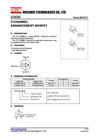
UNISONIC TECHNOLOGIES CO., LTD UT6302 Power MOSFET P-CHANNEL ENHANCEMENT MOSFET DESCRIPTION The UTC UT6302 is a power MOSFET offering the customers efficient and reliable performance. The UTC UT6302 is ideal for thin application environments, such as portable electronics and PCMCIA cards. FEATURES * Extremely-Low On-Resistance * Fast Switching Speed SYMBOL Drain (... See More ⇒
stk630f.pdf
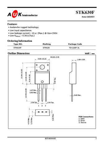
STK630F Semiconductor Semiconductor Power MOSFET Features Avalanche rugged technology. Low input capacitance. Low leakage current 10 (Max.) @ VDS=200V. Low RDS(on) 0.30 (Typ.) Ordering Information Type NO. Marking Package Code STK630F STK630 TO-220F-3L Outline Dimensions unit mm 3.05 3.35 9.80 10.20 2.60 3.00 1.07 Min. 0.90 Max. ... See More ⇒
snn0630q.pdf
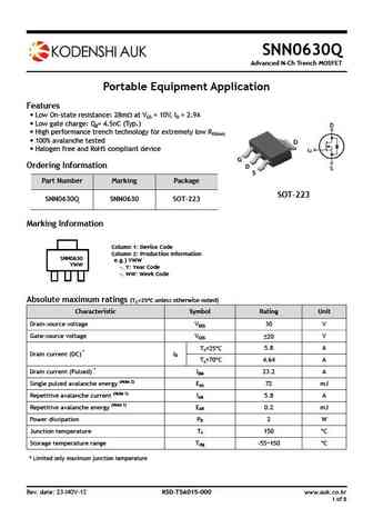
SNN0630Q Advanced N-Ch Trench MOSFET Portable Equipment Application Features Low On-state resistance 28m at VGS = 10V, ID = 2.9A Low gate charge Qg= 4.5nC (Typ.) High performance trench technology for extremely low RDS(on) 100% avalanche tested D Halogen free and RoHS compliant device G Ordering Information D S Part Number Marking Package S... See More ⇒
smn630ld.pdf
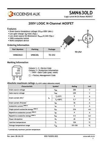
SMN630LD Logic Level N-Ch Power MOSFET 200V LOGIC N-Channel MOSFET Features Drain-Source breakdown voltage BV =200V (Min.) DSS Low gate charge Q =12nC (Typ.) g Low drain-source On-Resistance R =0.34 (Typ.) DS(on) D 100% avalanche tested RoHS compliant device Ordering Information G S Part Number Marking Package TO-252 SMN630LD SMN630L TO-... See More ⇒
smk630f.pdf
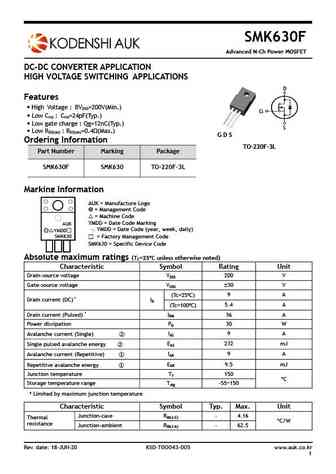
SMK630F Advanced N-Ch Power MOSFET DC-DC CONVERTER APPLICATION HIGH VOLTAGE SWITCHING APPLICATIONS Features High Voltage BV =200V(Min.) DSS Low C C =24pF(Typ.) rss rss Low gate charge Qg=12nC(Typ.) Low R R =0.4 (Max.) DS(on) DS(on) G D S Ordering Information TO-220F-3L Part Number Marking Package SMK630F SMK630 TO-220F-3L Marking Info... See More ⇒
smk630d.pdf
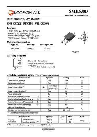
SMK630D Advanced N-Ch Power MOSFET DC-DC CONVERTER APPLICATION HIGH VOLTAGE SWITCHING APPLICATIONS Features High Voltage BVDSS=200V(Min.) D Low Crss Crss=24pF(Typ.) Low gate charge Qg=12nC(Typ.) Low RDS(on) RDS(on)=0.4 (Max.) Ordering Information G S Type No. Marking Package Code SMK630D SMK630 TO-252 TO-252 Marking Diagram SMK Co... See More ⇒
mrfe6vp6300h.pdf
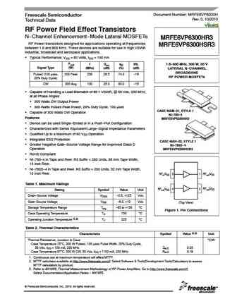
Document Number MRFE6VP6300H Freescale Semiconductor Rev. 0, 10/2010 Technical Data RF Power Field Effect Transistors N--Channel Enhancement--Mode Lateral MOSFETs MRFE6VP6300HR3 RF Power transistors designed for applications operating at frequencies MRFE6VP6300HSR3 between 1.8 and 600 MHz. These devices are suitable for use in high VSWR industrial, broadcast and aerospace application... See More ⇒
2n6306 2n6308.pdf
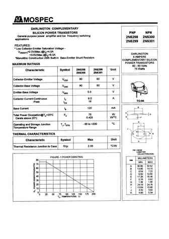
The documentation and process conversion INCH-POUND measures necessary to comply with this revision shall MIL-PRF-19500/498E be completed by 12 August 20005. 12 May 2005 SUPERSEDING MIL-PRF-19500/498D 30 April 2003 * PERFORMANCE SPECIFICATION SHEET SEMICONDUCTOR DEVICE, TRANSISTOR, NPN, SILICON, POWER, TYPES 2N6306, 2N6306T1, 2N6306T3, 2N6308, 2N6308T1, 2N6308T3, JAN, J... See More ⇒
mrf630.pdf
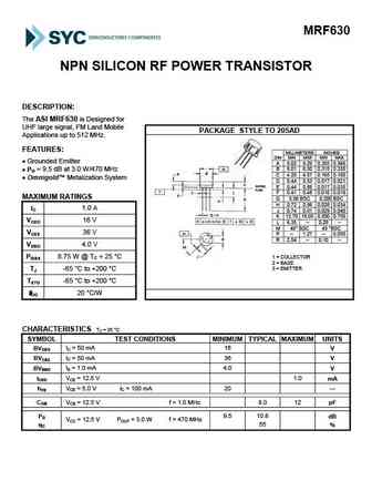
MRF630 NPN SILICON RF POWER TRANSISTOR DESCRIPTION The ASI MRF630 is Designed for UHF large signal, FM Land Mobile PACKAGE STYLE TO 205AD Applications up to 512 MHz. FEATURES MILLIMETERS INCHES DIM MIN MAX MIN MAX Grounded Emitter A 9.02 9.29 0.355 0.366 B 8.01 8.50 0.315 0.335 PG = 9.5 dB at 3.0 W/470 MHz C 4.20 4.57 0.165 0.180 Omnigold Metalization Sys... See More ⇒
sdt96305.pdf
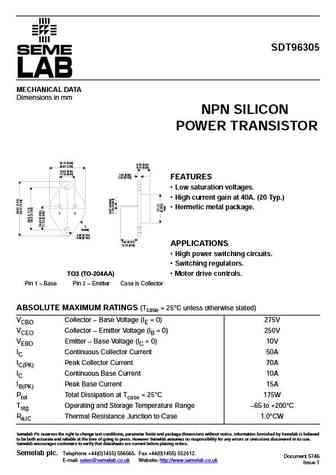
SDT96305 MECHANICAL DATA Dimensions in mm NPN SILICON POWER TRANSISTOR 25.15 (0.99) 6.35 (0.25) 26.67 (1.05) 9.15 (0.36) 10.67 (0.42) 11.18 (0.44) 1.52 (0.06) 3.43 (0.135) FEATURES Low saturation voltages. High current gain at 40A. (20 Typ.) Hermetic metal package. 1 2 3 (case) 3.84 (0.151) 4.09 (0.161) 7.92 (0.312) APPLICATIONS 12.70 (0.50) High power sw... See More ⇒
sdt96304.pdf
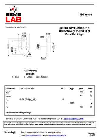
SDT96304 Dimensions in mm (inches). Bipolar NPN Device in a Hermetically sealed TO3 25.15 (0.99) 6.35 (0.25) 26.67 (1.05) 9.15 (0.36) Metal Package. 10.67 (0.42) 11.18 (0.44) 1.52 (0.06) 3.43 (0.135) 1 2 3 (case) 3.84 (0.151) 4.09 (0.161) 7.92 (0.312) 12.70 (0.50) TO3 (TO204AE) PINOUTS 1 Base 2 Emitter Case - Collector Parameter Test Conditions Min. Typ. M... See More ⇒
2n6299smd05 2n6299smd 2n6301smd 2n6301smd05.pdf
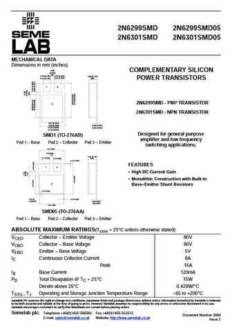
2N6299SMD 2N6299SMD05 2N6301SMD 2N6301SMD05 MECHANICAL DATA Dimensions in mm (inches) COMPLEMENTARY SILICON POWER TRANSISTORS 2N6299SMD - PNP TRANSISTOR 2N6301SMD - NPN TRANSISTOR Designed for general ... See More ⇒
2n6302.pdf
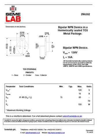
2N6302 Dimensions in mm (inches). Bipolar NPN Device in a Hermetically sealed TO3 25.15 (0.99) 6.35 (0.25) 26.67 (1.05) 9.15 (0.36) Metal Package. 10.67 (0.42) 11.18 (0.44) 1.52 (0.06) 3.43 (0.135) 1 2 Bipolar NPN Device. 3 VCEO = 120V (case) 3.84 (0.151) 4.09 (0.161) 7.92 (0.312) IC = 16A 12.70 (0.50) All Semelab hermetically sealed products can be processed in ... See More ⇒
2n6301smd05.pdf

2N6299SMD 2N6299SMD05 2N6301SMD 2N6301SMD05 MECHANICAL DATA Dimensions in mm (inches) COMPLEMENTARY SILICON POWER TRANSISTORS 2N6299SMD - PNP TRANSISTOR 2N6301SMD - NPN TRANSISTOR Designed for general ... See More ⇒
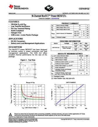
csd16301q2.pdf
CSD16301Q2 www.ti.com SLPS235C OCTOBER 2009 REVISED JULY 2011 N-Channel NexFET Power MOSFETs Check for Samples CSD16301Q2 1 FEATURES PRODUCT SUMMARY 2 Ultralow Qg and Qgd VDS Drain to Source Voltage 25 V Low Thermal Resistance Qg Gate Charge Total ( 4.5V) 2 nC Pb Free Terminal Plating Qgd Gate Charge Gate to Drain 0.4 nC RoHS Compliant VGS = 3V 27 m ... See More ⇒
kf630d-s kf621 kf622 kf520 kf521 kf522 kf523 kf552 kf907 kf910.pdf
... See More ⇒
2n5629 2n5630.pdf
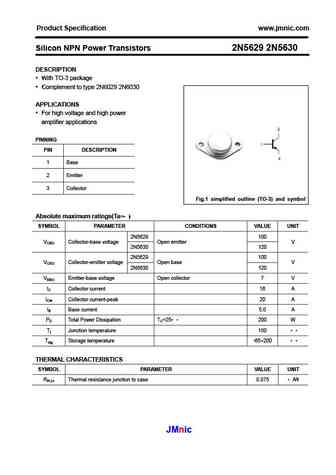
Product Specification www.jmnic.com Silicon NPN Power Transistors 2N5629 2N5630 DESCRIPTION With TO-3 package Complement to type 2N6029 2N6030 APPLICATIONS For high voltage and high power amplifier applications PINNING PIN DESCRIPTION 1 Base 2 Emitter 3 Collector Fig.1 simplified outline (TO-3) and symbol Absolute maximum ratings(Ta= ) SYMBOL PARAMETER CONDITIO... See More ⇒
2n6306 2n6308.pdf
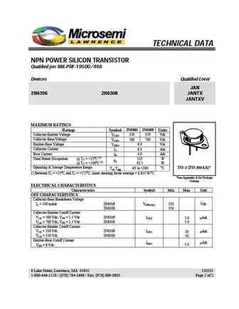
TECHNICAL DATA NPN POWER SILICON TRANSISTOR Qualified per MIL-PRF-19500/498 Devices Qualified Level JAN 2N6306 2N6308 JANTX JANTXV MAXIMUM RATINGS Ratings Symbol 2N6306 2N6308 Units Collector-Emitter Voltage 250 350 Vdc VCEO Collector-Base Voltage 500 700 Vdc VCBO Emitter-Base Voltage 8.0 Vdc VEBO Collector Current 8.0 Adc IC Base Current 4.0 Adc IB Total P... See More ⇒
2n6303.pdf
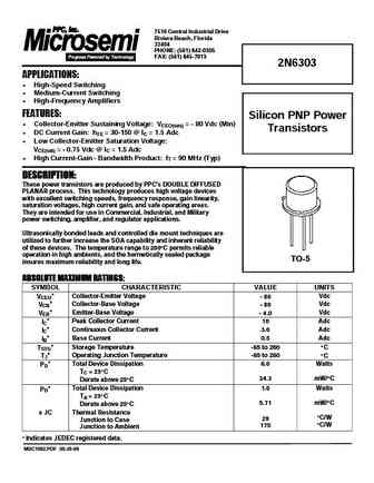
7516 Central Industrial Drive Riviera Beach, Florida 33404 PHONE (561) 842-0305 FAX (561) 845-7813 2N6303 APPLICATIONS High-Speed Switching Medium-Current Switching High-Frequency Amplifiers FEATURES Silicon PNP Power Collector-Emitter Sustaining Voltage VCEO(sus) = - 80 Vdc (Min) Transistors DC Current Gain hFE = 30-150 @ IC = 1.5 Adc Low Collector-... See More ⇒
2n6304.pdf
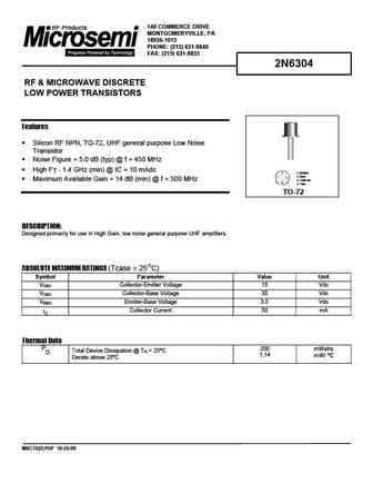
140 COMMERCE DRIVE MONTGOMERYVILLE, PA 18936-1013 PHONE (215) 631-9840 FAX (215) 631-9855 2N6304 RF & MICROWAVE DISCRETE LOW POWER TRANSISTORS Features Silicon RF NPN, TO-72, UHF general purpose Low Noise Transistor Noise Figure = 5.0 dB (typ) @ f = 450 MHz High FT - 1.4 GHz (min) @ IC = 10 mAdc 2 1. Emitter 2. Base 1 3 Maximum Available Gain = 14 dB (min) @ f... See More ⇒
cep630n ceb630n cef630n.pdf
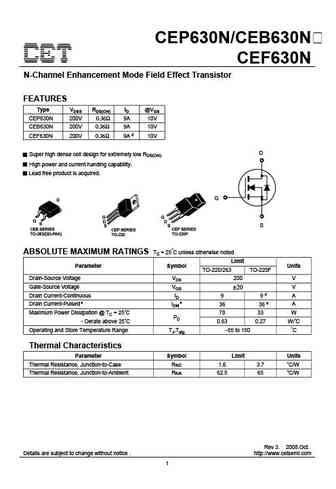
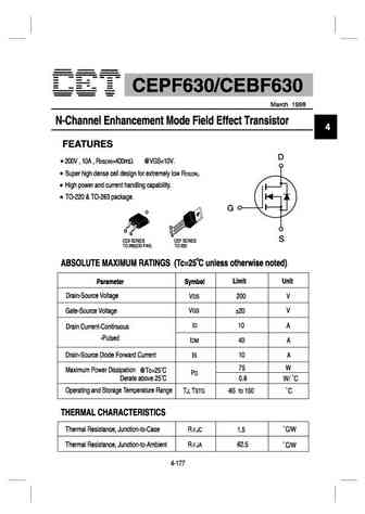
CEP630N/CEB630N CEF630N N-Channel Enhancement Mode Field Effect Transistor FEATURES Type VDSS RDS(ON) ID @VGS CEP630N 200V 0.36 9A 10V CEB630N 200V 0.36 9A 10V CEF630N 200V 0.36 9A d 10V D Super high dense cell design for extremely low RDS(ON). High power and current handing capability. Lead free product is acquired. G S CEB SERIES CEP SERIES CEF SERIES TO-263(DD-PAK) ... See More ⇒
ceu630n ced630n.pdf
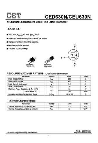
CED630N/CEU630N N-Channel Enhancement Mode Field Effect Transistor FEATURES 200V, 7.5A, RDS(ON) = 0.36 @VGS = 10V. Super high dense cell design for extremely low RDS(ON). High power and current handing capability. D Lead free product is acquired. TO-251 & TO-252 package. D G G S CEU SERIES CED SERIES S TO-252(D-PAK) TO-251(I-PAK) ABSOLUTE MAXIMUM RATINGS Tc = 25 C unless oth... See More ⇒
hirf630.pdf
Spec. No. MOS200401 HI-SINCERITY Issued Date 2004.04.01 Revised Date 2005.04.22 MICROELECTRONICS CORP. Page No. 1/6 HIRF630 Series Pin Assignment HIRF630 / HIRF630F Tab N-CHANNEL POWER MOSFET 3-Lead Plastic TO-220AB Package Code E Pin 1 Gate Pin 2 & Tab Drain Description Pin 3 Source This power MOSFET is designed for low voltage, high speed power switching applicati... See More ⇒
aonr26309a.pdf
AONR26309A 30V Complementary MOSFET General Description Product Summary N-channel P-channel The AONR26309A uses advanced trench technology to provide excellent RDS(ON) and low gate charge. The VDS (V) = 30V VDS (V) = -30V complementary MOSFETs may be used in inverter and ID = 14A ID = -21A (VGS = 10V) other applications. RDS(ON) ... See More ⇒
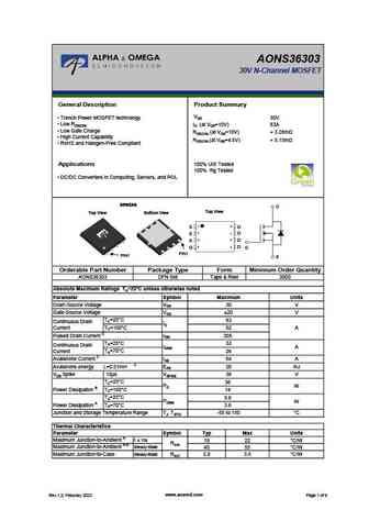
aons36308.pdf

AONS36308 30V N-Channel MOSFET General Description Product Summary VDS 30V Trench Power MOSFET technology Low RDS(ON) ID (at VGS=10V) 53A Low Gate Charge RDS(ON) (at VGS=10V) ... See More ⇒
aons36303.pdf
AONS36303 30V N-Channel MOSFET General Description Product Summary VDS Trench Power MOSFET technology 30V Low RDS(ON) ID (at VGS=10V) 83A Low Gate Charge RDS(ON) (at VGS=10V) ... See More ⇒
aons36302.pdf
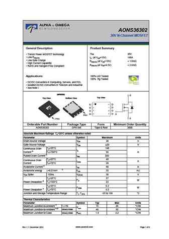
AONS36302 30V N-Channel MOSFET General Description Product Summary VDS 30V Trench Power MOSFET technology Low RDS(ON) ID (at VGS=10V) 146A Low Gate Charge RDS(ON) (at VGS=10V) ... See More ⇒
aons36304.pdf
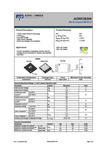
AONS36304 30V N-Channel MOSFET General Description Product Summary VDS 30V Trench Power MOSFET technology Low RDS(ON) ID (at VGS=10V) 85A Low Gate Charge RDS(ON) (at VGS=10V) ... See More ⇒
ao4630.pdf
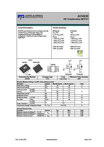
AO4630 30V Complementary MOSFET General Description Product Summary AO4630 uses advanced trench technology to provide N-Channel P-Channel excellent RDS(ON) and low gate charge. This VDS= 30V -30V complementary N and P channel MOSFET ID= 7A (VGS=10V) -5A (VGS=-10V) configuration is ideal for low Input Voltage inverter RDS(ON) RDS(ON) applications. ... See More ⇒
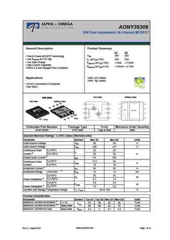
aony36302.pdf
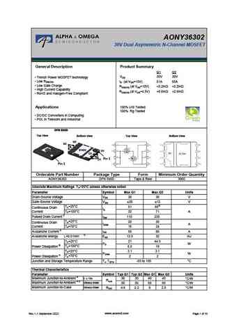
AONY36302 30V Dual Asymmetric N-Channel MOSFET General Description Product Summary Q1 Q2 VDS 30V 30V Trench Power MOSFET technology Low RDS(ON) ID (at VGS=10V) 51A 85A Low Gate Charge RDS(ON) (at VGS=10V) ... See More ⇒
aons36306.pdf
AONS36306 30V N-Channel MOSFET General Description Product Summary VDS 30V Trench Power MOSFET technology Low RDS(ON) ID (at VGS=10V) 63A Low Gate Charge RDS(ON) (at VGS=10V) ... See More ⇒
aony36306.pdf
AONY36306 30V Dual Asymmetric N-Channel MOSFET General Description Product Summary Q1 Q2 VDS 30V 30V Trench Power MOSFET technology Low RDS(ON) at 4.5V Vgs ID (at VGS=10V) 32A 32A Low Gate Charge RDS(ON) (at VGS=10V) ... See More ⇒
aony36304.pdf

AONY36304 30V Dual Asymmetric N-Channel MOSFET General Description Product Summary Q1 Q2 VDS 30V 30V Trench Power MOSFET technology Low RDS(ON) ID (at VGS=10V) 51A 85A Low Gate Charge RDS(ON) (at VGS=10V) ... See More ⇒
irf630.pdf
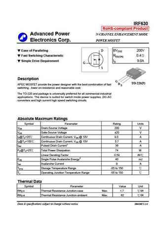
IRF630 RoHS-compliant Product Advanced Power N-CHANNEL ENHANCEMENT MODE Electronics Corp. POWER MOSFET Ease of Paralleling D BVDSS 200V Fast Switching Characteristic RDS(ON) 0.4 Simple Drive Requirement ID 9.0A G S Description G TO-220(P) D APEC MOSFET provide the power designer with the best combination of fast S switching , lower on-resistance and reasonable cost.... See More ⇒
am7630n.pdf
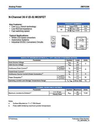
Analog Power AM7630N N-Channel 30-V (D-S) MOSFET PRODUCT SUMMARY Key Features rDS(on) (m ) VDS (V) ID (A) Low r trench technology DS(on) 19 @ VGS = 10V 9.4 Low thermal impedance 30 28 @ VGS = 4.5V 7.8 Fast switching speed Typical Applications White LED boost converters Automotive Systems Industrial DC/DC Conversion Circuits ABSOLUTE MAXIMUM ... See More ⇒
afn3630.pdf
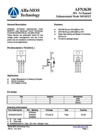
AFN3630 Alfa-MOS 30V N-Channel Technology Enhancement Mode MOSFET General Description Features AFN3630, N-Channel enhancement mode 30V/20A,RDS(ON)=30m @VGS=10V MOSFET, uses Advanced Trench Technology 30V/15A,RDS(ON)=38m @VGS=4.5V to provide excellent RDS(ON), low gate charge. Super high density cell design for extremely These devices are particularly suited for lo... See More ⇒
jcs630va jcs630ra jcs630va jcs630ba jcs630sa jcs630fa jcs630ca.pdf
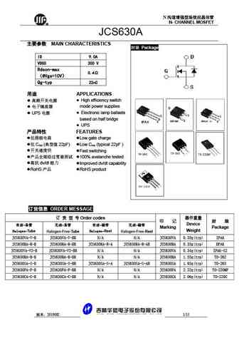
N N- CHANNEL MOSFET R JCS630A MAIN CHARACTERISTICS Package ID 9.0A VDSS 200 V Rdson-max 0.4 @Vgs=10V Qg-typ 22nC APPLICATIONS High efficiency switch mode power supplies Electronic lamp ballasts UPS based on half bridge ... See More ⇒
jcs630va jcs630ra jcs630ba jcs630sa jcs630ca jcs630fa.pdf
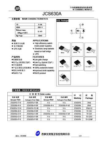
N N- CHANNEL MOSFET R JCS630A MAIN CHARACTERISTICS Package ID 9.0A VDSS 200 V Rdson-max 0.4 @Vgs=10V Qg-typ 22nC APPLICATIONS High efficiency switch mode power supplies Electronic lamp ballasts UPS based on half bridge ... See More ⇒
mtdn6303s6r.pdf
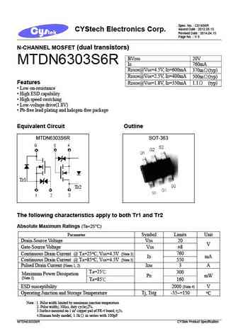
Spec. No. C814S6R Issued Date 2012.05.15 CYStech Electronics Corp. Revised Date 2014.04.15 Page No. 1/ 8 N-CHANNEL MOSFET (dual transistors) BVDSS 20V MTDN6303S6R ID 760mA RDSON@VGS=4.5V, ID=600mA 370m (typ) RDSON@VGS=2.5V, ID=400mA 500m (typ) Features RDSON@VGS=1.8V, ID=350mA 1.1 (typ) Low on-resistance High ESD capability High speed switching... See More ⇒
630a.pdf
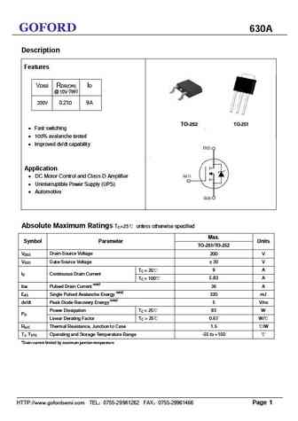
GOFORD 630A Description Features VDSS RDS(ON) ID @ 10V (typ) 9A 200V 0.21 TO-252 TO-251 Fast switching 100% avalanche tested Improved dv/dt capability Application DC Motor Control and Class D Amplifier Uninterruptible Power Supply (UPS) Automotive Absolute Maximum Ratings TC=25 unless otherwise specified Max. Symbol Parameter Unit... See More ⇒
stu630s.pdf
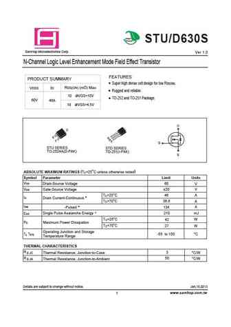
Green Product STU/D630S SamHop Microelectronics Corp. Ver 1.0 N-Channel Logic Level Enhancement Mode Field Effect Transistor FEATURES PRODUCT SUMMARY Super high dense cell design for low RDS(ON). RDS(ON) (m ) Max VDSS ID Rugged and reliable. 10 @VGS=10V TO-252 and TO-251 Package. 60V 46A 18 @VGS=4.5V G S STU SERIES STD SERIES TO-252AA(D-PAK) TO-251(I-PAK) ABSOLUTE MAXIMU... See More ⇒
sts6308.pdf
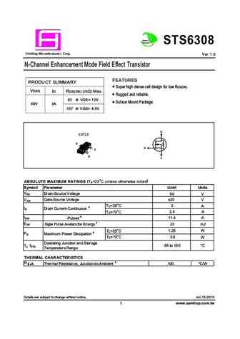
Green Product STS6308 a S mHop Microelectronics C orp. Ver 1.0 N-Channel Enhancement Mode Field Effect Transistor FEATURES PRODUCT SUMMARY Super high dense cell design for low RDS(ON). VDSS ID RDS(ON) (m ) Max Rugged and reliable. 83 @ VGS= 10V Suface Mount Package. 60V 3A 107 @ VGS= 4.5V D S OT23 D G S G S (TA=25 C unless otherwise noted) ABSOLUTE MAXIMUM RATINGS Sy... See More ⇒
vti630f.pdf
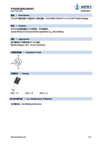
VTI630F(BRCS630F) Rev.C Feb.-2015 DATA SHEET / Descriptions TO-220F N MOS N-CHANNEL MOSFET in a TO-220F Plastic Package. / Features RDS(on) 0.3 , Typical RDS(on)=0.3 ,low intrinsic capacitance Ciss, fast switching. / Applications , ,DC-DC ... See More ⇒
bri630.pdf
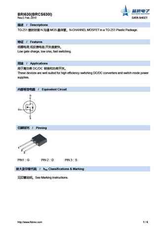
BRI630(BRCS630I) Rev.C Feb.-2015 DATA SHEET / Descriptions TO-251 N MOS N-CHANNEL MOSFET in a TO-251 Plastic Package. / Features , , Low gate charge, low crss, fast switching. / Applications DC/DC These devices are well suited for high effi... See More ⇒
brcs630fa.pdf
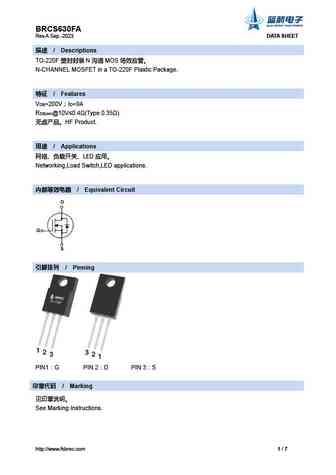
BRCS630FA Rev.A Sep.-2023 DATA SHEET / Descriptions TO-220F N MOS N-CHANNEL MOSFET in a TO-220F Plastic Package. / Features V =200V I =9A DS D R DS(on)@10V 0.4 (Type.0.35 ) HF Product. / Applications LED Networking,Load Switch,LED applications. ... See More ⇒
vti630.pdf
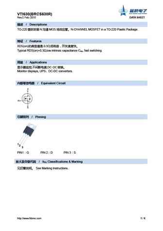
VTI630(BRCS630R) Rev.C Feb.-2015 DATA SHEET / Descriptions TO-220 N MOS N-CHANNEL MOSFET in a TO-220 Plastic Package. / Features RDS(on) 0.3 , Typical RDS(on)=0.3 ,low intrinsic capacitance Ciss, fast switching. / Applications , ,DC-DC ... See More ⇒
brd630.pdf
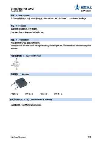
BRD630(BRCS630D) Rev.C Feb.-2015 DATA SHEET / Descriptions TO-252 N MOS N-CHANNEL MOSFET in a TO-252 Plastic Package. / Features , , Low gate charge, low crss, fast switching. / Applications DC/DC These devices are well suited for high e... See More ⇒
irf630h.pdf
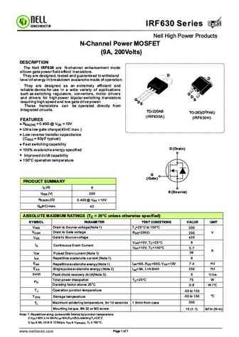
RoHS IRF630 Series RoHS SEMICONDUCTOR Nell High Power Products N-Channel Power MOSFET (9A, 200Volts) DESCRIPTION The Nell IRF630 are N-channel enhancement mode silicon gate power field effect transistors. D They are designed, tested and guaranteed to withstand D level of energy in breakdown avalanche made of operation. They are designed as an extremely efficient and reliab... See More ⇒
hfp630.pdf
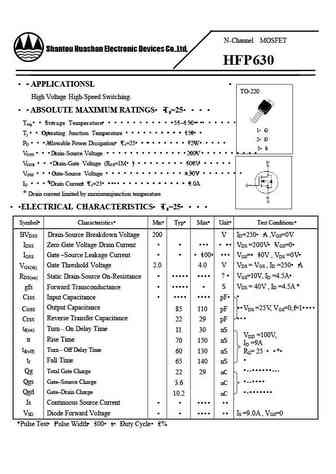
N-Channel MOSFET Shantou Huashan Electronic Devices Co.,Ltd. HFP630 APPLICATIONSL TO-220 High Voltage High-Speed Switching. ABSOLUTE MAXIMUM RATINGS Ta=25 Tstg Storage Temperature -55 150 1 G Tj Operating Junction Temperature 150 2 D PD Allowable Power Dissipation ... See More ⇒
hff630.pdf
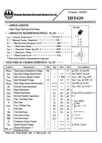
N-Channel MOSFET Shantou Huashan Electronic Devices Co.,Ltd. HFF630 APPLICATIONSL TO-220F High Voltage High-Speed Switching. ABSOLUTE MAXIMUM RATINGS Ta=25 1 Tstg Storage Temperature -55 150 1 G Tj Operating Junction Temperature 150 2 D PD Allowable Power Dissipatio... See More ⇒
sm2630dsc.pdf
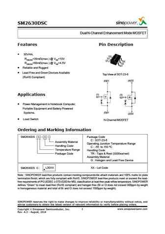
SM2630DSC Dual N-Channel Enhancement Mode MOSFET Features Pin Description 30V/4A, D2 S1 RDS(ON)=39m (max.) @ VGS=10V D1 G2 RDS(ON)=68m (max.) @ VGS=4.5V S2 G1 Reliable and Rugged Lead Free and Green Devices Available Top View of SOT-23-6 (RoHS Compliant) (6)D1 (4)D2 (1) (3) Applications G1 G2 Power Management in Notebook Computer, Portable Equipment and Ba... See More ⇒
cs630 a8h.pdf
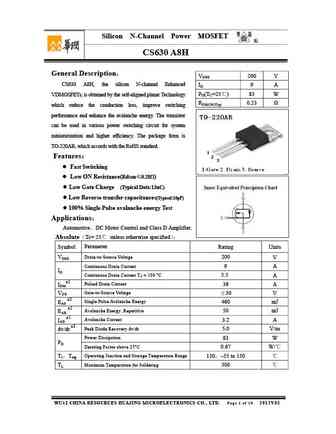
Silicon N-Channel Power MOSFET R CS630 A8H General Description VDSS 200 V CS630 A8H, the silicon N-channel Enhanced ID 9 A PD(TC=25 ) 83 W VDMOSFETs, is obtained by the self-aligned planar Technology RDS(ON)Typ 0.23 which reduce the conduction loss, improve switching performance and enhance the avalanche energy. The transistor can be used in various power sw... See More ⇒
cs630 a3h.pdf

Silicon N-Channel Power MOSFET R CS630 A3H General Description VDSS 200 V CS630 A3H, the silicon N-channel Enhanced VDMOSFETs, is ID 9 A PD(TC=25 ) 83 W obtained by the self-aligned planar Technology which reduce the RDS(ON)Typ 0.23 conduction loss, improve switching performance and enhance the avalanche energy. The transistor can be used in various power swi... See More ⇒
cs630 a4h.pdf
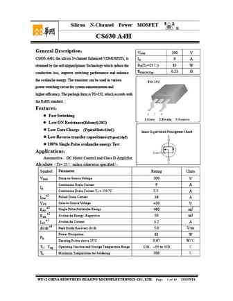
Silicon N-Channel Power MOSFET R CS630 A4H General Description VDSS 200 V CS630 A4H, the silicon N-channel Enhanced VDMOSFETs, is ID 9 A PD(TC=25 ) 83 W obtained by the self-aligned planar Technology which reduce the RDS(ON)Typ 0.23 conduction loss, improve switching performance and enhance the avalanche energy. The transistor can be used in various power swi... See More ⇒
cs630f a9h.pdf
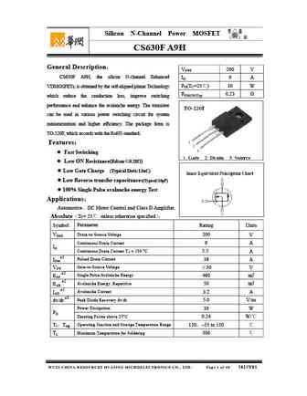
Silicon N-Channel Power MOSFET R CS630F A9H General Description VDSS 200 V CS630F A9H, the silicon N-channel Enhanced ID 9 A PD(TC=25 ) 30 W VDMOSFETs, is obtained by the self-aligned planar Technology RDS(ON)Typ 0.23 which reduce the conduction loss, improve switching performance and enhance the avalanche energy. The transistor can be used in various power... See More ⇒
cs5630.pdf
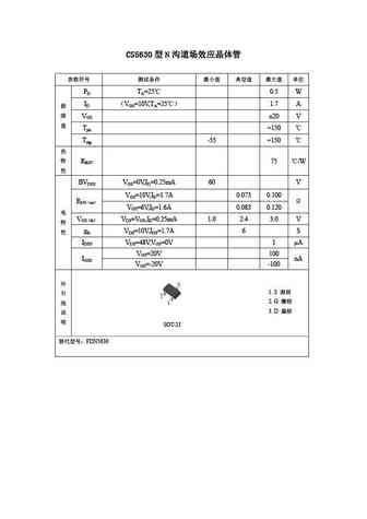
CS5630 N PD TA=25 0.5 W ID VGS=10V,TA=25 1.7 A VGS 20 V Tjm +150 Tstg -55 +150 RthJC 75 /W BVDSS VGS=0V,ID=0.25mA 60 V VGS=10V,ID=1.7A 0.073 0.100 RDS on VGS=6V,ID=1.6A 0.083 0.120 VGS th VDS=VGS,ID=0.25mA 1.0 2.4 3.0... See More ⇒
irlml6302.pdf
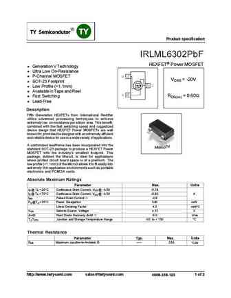
Product specification IRLML6302PbF HEXFET Power MOSFET l Generation V Technology l Ultra Low On-Resistance l P-Channel MOSFET VDSS = -20V l SOT-23 Footprint l Low Profile (... See More ⇒
kqb630.pdf
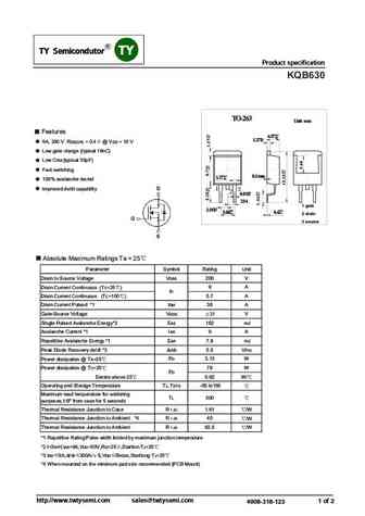
SMD Type IC SMD Type Transistors Product specification KQB630 TO-263 Unit mm Features 4.57+0.2 -0.2 +0.1 1.27-0.1 9A, 200 V. RDS(ON) =0.4 @VGS =10 V Low gate charge (typical 19nC) Low Crss(typical 35pF) Fast switching +0.1 0.1max 1.27-0.1 100% avalanche tested lmproved dv/dt capability 0.81+0.1 -0.1 2.54 1gate 1Gate 2.54+0.2 +0.2 -0.2 +0.1 5.08-0.1 0.4-0.2 2drain 2... See More ⇒
ftk630 ftk630p f.pdf
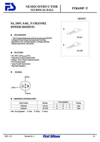
SEMICONDUCTOR FTK630P / F TECHNICAL DATA MOSFET 9A, 200V, 0.4 , N-CHANNEL POWER MOSFETS P 1 DESCRIPTION TO-220 The N-Channel enhancement mode silicon gate power MOSFET is designed for high voltage, high speed power switching applications such as switching regulators, switching converters, solenoid, motor drivers, relay drivers. F 1 TO-220F FEATURES * 9A, 200V, Low RDS(ON... See More ⇒
brd630.pdf
SEMICONDUCTOR BRD630 TECHNICAL DATA N-Channel Power MOSFET A I C J GENERAL DESCRIPTION DIM MILLIMETERS This advanced high voltage MOSFET is designed to stand high A 6 50 0 2 B 5 60 0 2 C 5 20 0 2 energy in the avalanche mode and switch efficiently. D 1 50 0 2 E 2 70 0 2 F 2 30 0 1 This new high energy device also offers a drain H H 1 00 MAX I 2 30 ... See More ⇒
fdg6301n.pdf
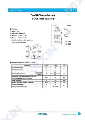
SMD Type MOSFET Dual N-Channel MOSFET FDG6301N (KDG6301N) Features VDS (V) = 25V ID = 220m A (VGS = 4.5V) RDS(ON) 4 (VGS = 4.5V) RDS(ON) 5 (VGS = 2.7V) Gate-Source Zener for ESD ruggedness 1 S 1 S1 4 S2 (>6kV Human Body Model). 2 G1 2 G1 5 G2 3 D2 3 D2 6 D1 1 or 4 6 or 3 2 or 5 5 or 2 4 or 1 3 or 6 Absolute Maximum Ratings T... See More ⇒
irf630s.pdf
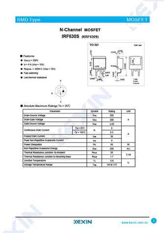
SMD Type MOSFET N-Channel MOSFET IRF630S (KRF630S) Features VDS (V) = 200V ID = 9 A (VGS = 10V) RDS(ON) 400m (VGS = 10V) Fast switching Low thermal resistance d g s Absolute Maximum Ratings Ta = 25 Parameter Symbol Rating Unit Drain-Source Voltage VDS 200 V Drain-Gate Voltage VDG 200 Gate-Source Voltage VGS 20 Ta = 25 9 Cont... See More ⇒
fdn5630-3.pdf

SMD Type MOSFET N-Channel MOSFET FDN5630 (KDN5630) SOT-23-3 Unit mm +0.2 2.9-0.1 +0.1 0.4 -0.1 3 Features VDS (V) = 60V ID = 1.7 A (VGS = 10V) 1 2 RDS(ON) 100m (VGS = 10V) +0.02 +0.1 0.15 -0.02 0.95 -0.1 +0.1 1.9-0.2 RDS(ON) 120m (VGS = 6V) 1. Gate D 2. Source 3. Drain G S Absolute Maximum Ratings Ta = 25 Parameter Symbol Ra... See More ⇒
fdn5630.pdf
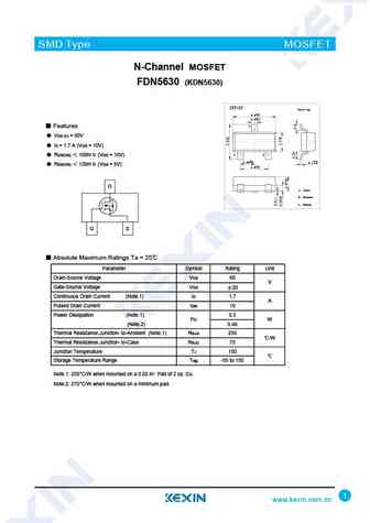
SMD Type MOSFET N-Channel MOSFET FDN5630 (KDN5630) SOT-23 Unit mm +0.1 2.9 -0.1 +0.1 0.4 -0.1 3 Features VDS (V) = 60V ID = 1.7 A (VGS = 10V) 1 2 RDS(ON) 100m (VGS = 10V) +0.1 +0.05 0.95-0.1 0.1-0.01 RDS(ON) 120m (VGS = 6V) +0.1 1.9-0.1 D 1. Gate 2. Source 3. Drain G S Absolute Maximum Ratings Ta = 25 Parameter Symbol Rating... See More ⇒
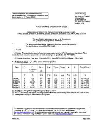
2n6300 2n6301.pdf
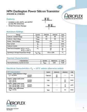
NPN Darlington Power Silicon Transistor 2N6300 & 2N6301 Features Available in JAN, JANTX, and JANTXV per MIL-PRF-19500/539 TO-66 (TO-213AA) Package Maximum Ratings Ratings Symbol 2N6300 2N6301 Units Collector - Emitter Voltage VCEO 60 80 Vdc Collector - Base Voltage VCBO 60 80 Vdc Emitter - Base Voltage VEBO 5.0 Vdc Base Current IB 120 mAdc Collector Current IC 8.0 Adc Tot... See More ⇒
wff630.pdf
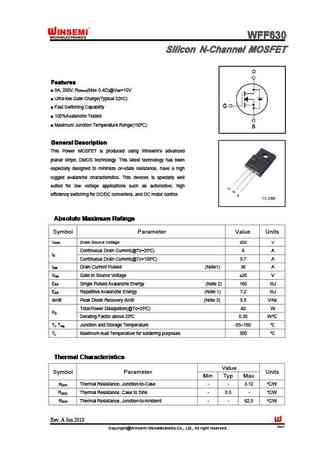
WFF630 WFF630 WFF630 WFF630 Silicon N-Channel MOSFET Silicon N-Channel MOSFET Silicon N-Channel MOSFET Silicon N-Channel MOSFET Features Features Features Features 9A, 200V, R (Max 0.4 )@V =10V DS(on) GS Ultra-low Gate Charge(Typical 22nC) Fast Switching Capability 100%Avalanche Tested Maximum Junction Temperature Range(150 ) General Description General... See More ⇒
sfp630.pdf
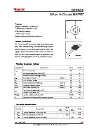
SFP630 Silicon N-Channel MOSFET Silicon N-Channel MOSFET Silicon N-Channel MOSFET Silicon N-Channel MOSFET Features Features Features Features 9A, 200V,RDS(on)(Max 0.4 )@VGS=10V Ultra-low Gate Charge(Typical 43nC) Fast Switching Capability 100%Avalanche Tested Maximum Junction Temperature Range(150 ) General Description General Description General Descript... See More ⇒
wfp630.pdf
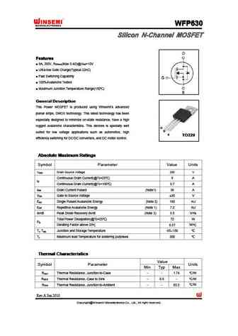
WFP630 WFP630 WFP630 WFP630 Silicon N-Channel MOSFET Silicon N-Channel MOSFET Silicon N-Channel MOSFET Silicon N-Channel MOSFET Features Features Features Features 9A, 200V, R (Max 0.4 )@V =10V DS(on) GS Ultra-low Gate Charge(Typical 22nC) Fast Switching Capability 100%Avalanche Tested Maximum Junction Temperature Range(150 ) General Description General... See More ⇒
chm630pagp.pdf
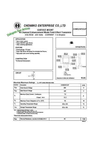
CHENMKO ENTERPRISE CO.,LTD CHM630PAGP SURFACE MOUNT N-Channel Enhancement Mode Field Effect Transistor VOLTAGE 200 Volts CURRENT 7.8 Ampere APPLICATION * Servo motor control. * Power MOSFET gate drivers. * Other switching applications. D-PAK(TO-252) FEATURE * Small package. (TO-252) * Super high dense cell design for extremely low RDS(ON). .094 (2.40) .280 (7.10) * High power... See More ⇒
chm6308sgp.pdf
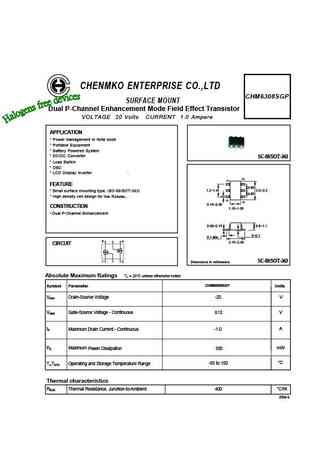
CHENMKO ENTERPRISE CO.,LTD CHM6308SGP SURFACE MOUNT Dual P-Channel Enhancement Mode Field Effect Transistor VOLTAGE 20 Volts CURRENT 1.0 Ampere APPLICATION * Power Management in Note book * Portable Equipment * Battery Powered System * DC/DC Converter SC-88/SOT-363 * Load Switch * DSC . * LCD Display inverter (6) (1) FEATURE 0.65 1.2 1.4 2.0 2.2 * Small surface mounting ... See More ⇒
fhu630a fhd630a fhp630a fhf630a.pdf
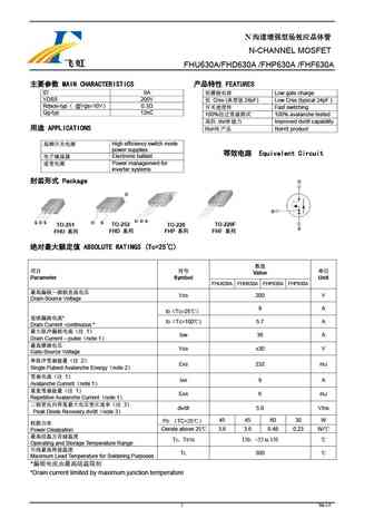
N N-CHANNEL MOSFET FHU630A/FHD630A /FHP630A /FHF630A MAIN CHARACTERISTICS FEATURES ID 9A Low gate charge VDSS 200V Crss ( 24pF) Low Crss (typical 24pF ) Rdson-typ @Vgs=10V 0.3 Fast switching Qg-typ 12nC 100% 100% avalanche tested dv/d... See More ⇒
kne6303a.pdf
12A, 30V N-CHANNELMOSFET KNX6303A KIA KIA KIA SEMICONDUCTORS SEMICONDUCTORS SEMICONDUCTORS 1.Features Advanced trenchprocess technology High density cell design for ultra lowon-resistance Fully characterized avalanche voltage and current 2.Applications Vds=30V R =9.0m (typ.),VGS@10V,Ids@12A DS(ON) R =11.5m (typ.),VGS@4.5V,Ids@6A DS(ON) 3. Pinconfiguration Pin Functio... See More ⇒
mg06300d-bn4mm.pdf
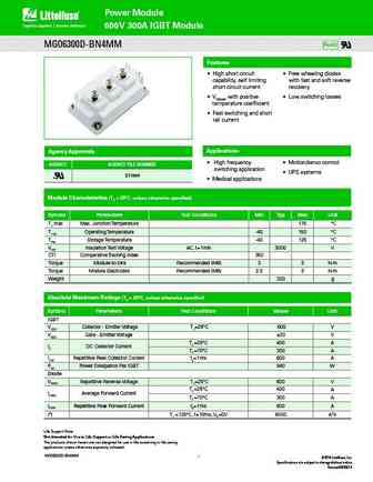
Power Module 600V 300A IGBT Module RoHS MG06300D-BN4MM Features High short circuit Free wheeling diodes capability, self limiting with fast and soft reverse short circuit current recovery VCE(sat) with positive Low switching losses temperature coefficient Fast switching and short tail current Applications Agency Approvals High frequency Motion/se... See More ⇒
cs630.pdf
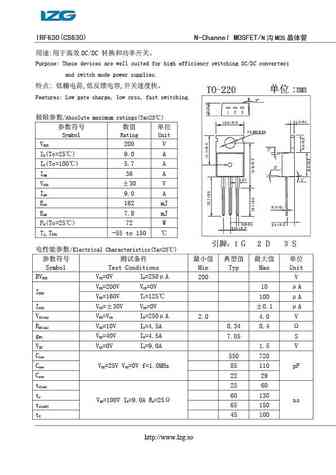
IRF630(CS630) N-Channel MOSFET/N MOS DC/DC Purpose These devices are well suited for high efficiency switching DC/DC converters and switch mode power supplies. , , Features Low gate charge, low crss, fast switching. /Absolute maximum ratings(Ta=25 ) ... See More ⇒
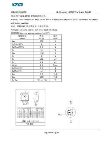
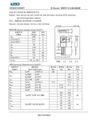
mee7630-g.pdf
Preliminary MEE7630-G N-Channel 40-V(D-S) MOSFET GENERAL DESCRIPTION FEATURES The MEE7630-G is the N-Channel enhancement mode power RDS(ON) 1.6m @VGS=10V field effect transistor, using Force-MOS patented Fast Trench Gate(FTG) RDS(ON) 2.6m @VGS=4.5V technology. This advanced technology is especially tailored to minimize Low Gate Charge on-state resistance and gate ... See More ⇒
sw630d swp630d swd630d.pdf

SW630D N-channel Enhanced mode TO-220/TO-252 MOSFET Features TO-220 TO-252 BVDSS 200V High ruggedness ID 9A Low RDS(ON) (Typ 0.27 )@VGS=10V RDS(ON) 0.27 Low Gate Charge (Typ 20nC) Improved dv/dt Capability 2 100% Avalanche Tested 1 1 2 2 Application Synchronous Rectification, 3 3 DC-DC 1 1. Gate 2. Drain 3. Source 3 G... See More ⇒
sw630 swp630 swf630 swd630.pdf
SAMWIN SW630 N-channel MOSFET TO-220F TO-220 TO-252 Features BVDSS 200V High ruggedness ID 10A RDS(ON) (Max 0.4 )@VGS=10V Gate Charge (Typ 20nC) RDS(ON) 0.4ohm 1 Improved dv/dt Capability 2 100% Avalanche Tested 1 1 3 2 2 3 3 2 1. Gate 2. Drain 3. Source General Description 1 This power MOSFET is produced with advanced VDMOS technology of SAMW... See More ⇒
swp630a1.pdf
SW630A1 N-channel Enhanced mode TO-220 MOSFET TO-220 BVDSS 200V Features ID 10A High ruggedness RDS(ON) 0.34 Low RDS(ON) (Typ 0.34 )@VGS=10V Low Gate Charge (Typ 17nC) 2 Improved dv/dt Capability 1 100% Avalanche Tested 2 1 3 Application LED , Charger, PC Power 1. Gate 2. Drain 3. Source 3 General Description This power... See More ⇒
swp630d swd630d.pdf
SW630D N-channel Enhanced mode TO-220/TO-252 MOSFET Features TO-220 TO-252 BVDSS 200V High ruggedness ID 9A Low RDS(ON) (Typ 0.27 )@VGS=10V RDS(ON) 0.27 Low Gate Charge (Typ 20nC) Improved dv/dt Capability 2 100% Avalanche Tested 1 1 2 2 Application Synchronous Rectification, 3 3 DC-DC 1 1. Gate 2. Drain 3. Source 3 G... See More ⇒
hfs630.pdf
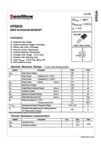
July 2005 BVDSS = 200 V RDS(on) typ HFS630 ID = 9 A 200V N-Channel MOSFET TO-220F FEATURES 1 Originative New Design 2 3 Superior Avalanche Rugged Technology 1.Gate 2. Drain 3. Source Robust Gate Oxide Technology Very Low Intrinsic Capacitances Excellent Switching Characteristics Unrivalled Gate Charge 22 nC (Typ.) Extended Safe Operating Area Lower RDS(ON... See More ⇒
hfd630 hfu630.pdf
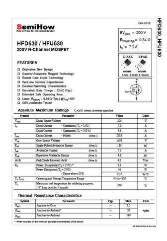
Dec 2012 BVDSS = 200 V RDS(on) typ HFD630 / HFU630 ID = 7.2 A 200V N-Channel MOSFET D-PAK I-PAK 2 FEATURES 1 1 3 2 3 Originative New Design HFD630 HFU630 Superior Avalanche Rugged Technology 1.Gate 2. Drain 3. Source Robust Gate Oxide Technology Very Low Intrinsic Capacitances Excellent Switching Characteristics Unrivalled Gate Charge 22 nC (Typ.) ... See More ⇒
shd226303.pdf
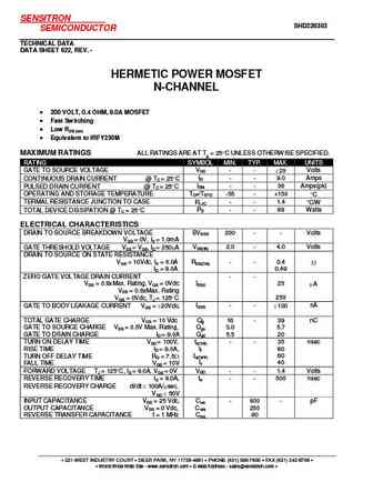
SENSITRON SHD226303 SEMICONDUCTOR TECHNICAL DATA DATA SHEET 622, REV. - HERMETIC POWER MOSFET N-CHANNEL 200 VOLT, 0.4 OHM, 9.0A MOSFET Fast Switching Low RDS (on) Equivalent to IRFY230M MAXIMUM RATINGS ALL RATINGS ARE AT TA = 25 C UNLESS OTHERWISE SPECIFIED. RATING SYMBOL MIN. TYP. MAX. UNITS GATE TO SOURCE VOLTAGE VGS - - 20 Volts ID - - 9.0 Amps CONTINUOUS DR... See More ⇒
shd226305 shd226305b.pdf
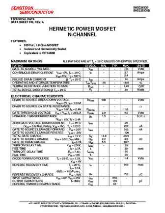
SHD226305 SENSITRON SHD226305B SEMICONDUCTOR TECHNICAL DATA DATA SHEET 336, REV. A HERMETIC POWER MOSFET N-CHANNEL FEATURES 500 Volt, 1.6 Ohm MOSFET Isolated and Hermetically Sealed Equivalent to IRFY430M MAXIMUM RATINGS ALL RATINGS ARE AT TA = 25 C UNLESS OTHERWISE SPECIFIED. RATING SYMBOL MIN. TYP. MAX. UNITS GATE TO SOURCE VOLTAGE VGS - - 20 Volts ID - - 3.7 A... See More ⇒
shd226302.pdf
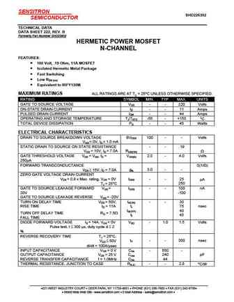
SENSITRON SHD226302 SEMICONDUCTOR TECHNICAL DATA DATA SHEET 222, REV. B Formerly Part Number SHD22632 HERMETIC POWER MOSFET N-CHANNEL FEATURES 100 Volt, .19 Ohm, 11A MOSFET Isolated Hermetic Metal Package Fast Switching Low RDS (on) Equivalent to IRFY130M MAXIMUM RATINGS ALL RATINGS ARE AT TC = 25 C UNLESS OTHERWISE SPECIFIED. RATING SYMBOL M... See More ⇒
shd226309.pdf
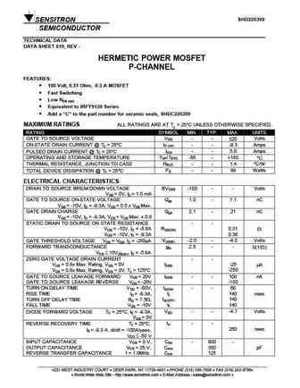
SHD226309 SENSITRON SEMICONDUCTOR TECHNICAL DATA DATA SHEET 619, REV - HERMETIC POWER MOSFET P-CHANNEL FEATURES 100 Volt, 0.31 Ohm, -9.3 A MOSFET Fast Switching Low RDS (on) Equivalent to IRFY9130 Series Add a C to the part number for ceramic seals, SHDC226309 MAXIMUM RATINGS ALL RATINGS ARE AT TC = 25 C UNLESS OTHERWISE SPECIFIED. RATIN... See More ⇒
ssm630gp.pdf
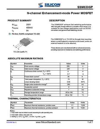
SSM630GP N-channel Enhancement-mode Power MOSFET PRODUCT SUMMARY DESCRIPTION The SSM630GP achieves fast switching performance BVDSS 200V with low gate charge without a complex drive circuit. It is RDS(ON) 400m suitable for low voltage applications such as DC/DC converters and general load-switching circuits. I 9A D Pb-free; RoHS-compliant TO-220 The SSM630GP is in TO-220 for thr... See More ⇒
stn6303.pdf
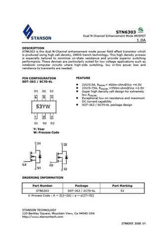
STN6303 Dual N Channel Enhancement Mode MOSFET 1.0A DESCRIPTION STN6303 is the dual N-Channel enhancement mode power field effect transistor which is produced using high cell density, DMOS trench technology. This high density process is especially tailored to minimize on-state resistance and provide superior switching performance. These devices are particularly suited for low volta... See More ⇒
stp6308.pdf
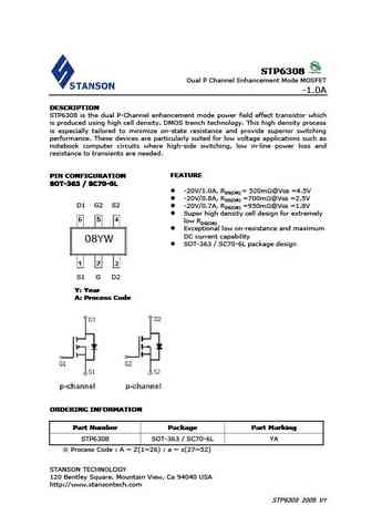
STP6308 STP6308 STP6308 STP6308 Dual P Channel Enhancement Mode MOSFET -1.0A DESCRIPTION DESCRIPTION DESCRIPTION DESCRIPTION STP6308 is the dual P-Channel enhancement mode power field effect transistor which is produced using high cell density, DMOS trench technology. This high density process is especially tailored to minimize on-state resistance and provide superior switching per... See More ⇒
stc6301d.pdf
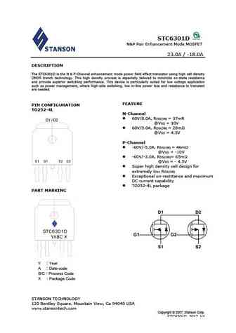
STC6301D N&P Pair Enhancement Mode MOSFET 23.0A / -18.0A DESCRIPTION The STC6301D is the N & P-Channel enhancement mode power field effect transistor using high cell density DMOS trench technology. This high density process is especially tailored to minimize on-state resistance and provide superior switching performance. This device is particularly suited for low voltage applicati... See More ⇒
tmp630z tmpf630z.pdf
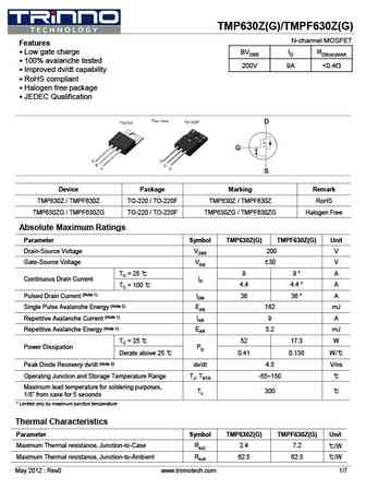
TMP630Z(G)/TMPF630Z(G) N-channel MOSFET Features Low gate charge BVDSS ID RDS(on)MAX 100% avalanche tested 200V 9A ... See More ⇒
tmd630z tmu630z.pdf
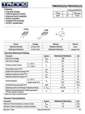
TMD630Z(G)/TMU630Z(G) Features N-channel MOSFET Low gate charge BVDSS ID RDS(on)MAX 100% avalanche tested 200V 9A ... See More ⇒
qm6301s.pdf
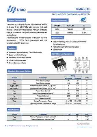
QM6301S N-Ch and P-Ch Fast Switching MOSFETs General Description Product Summery The QM6301S is the highest performance trench BVDSS RDSON ID N-ch and P-ch MOSFETs with extreme high cell 60V 30m 8A density , which provide excellent RDSON and gate charge for most of the synchronous buck converter -60V 60m -5.7A applications . Applications The QM6301S meet the RoHS and ... See More ⇒
cs630a3h.pdf
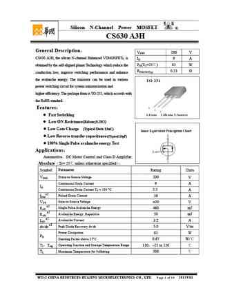
Silicon N-Channel Power MOSFET R CS630 A3H General Description VDSS 200 V CS630 A3H, the silicon N-channel Enhanced VDMOSFETs, is ID 9 A PD(TC=25 ) 83 W obtained by the self-aligned planar Technology which reduce the RDS(ON)Typ 0.23 conduction loss, improve switching performance and enhance the avalanche energy. The transistor can be used in various power swi... See More ⇒
cs630fa9h.pdf
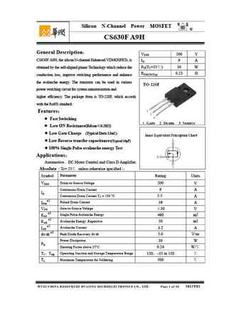
Silicon N-Channel Power MOSFET R CS630F A9H General Description VDSS 200 V CS630F A9H, the silicon N-channel Enhanced VDMOSFETs, is ID 9 A PD(TC=25 ) 30 W obtained by the self-aligned planar Technology which reduce the RDS(ON)Typ 0.23 conduction loss, improve switching performance and enhance the avalanche energy. The transistor can be used in various power... See More ⇒
cs630a4h.pdf
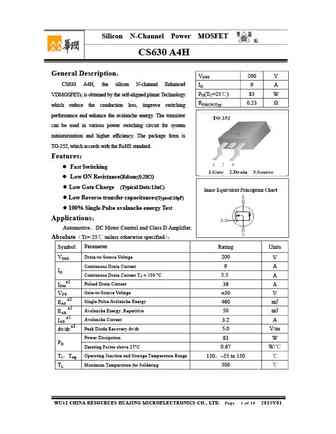
Silicon N-Channel Power MOSFET R CS630 A4H General Description VDSS 200 V CS630 A4H, the silicon N-channel Enhanced ID 9 A PD(TC=25 ) 83 W VDMOSFETs, is obtained by the self-aligned planar Technology RDS(ON)Typ 0.23 which reduce the conduction loss, improve switching performance and enhance the avalanche energy. The transistor can be used in various power swi... See More ⇒
cs630a8h.pdf

Silicon N-Channel Power MOSFET R CS630 A8H General Description VDSS 200 V CS630 A8H, the silicon N-channel Enhanced ID 9 A PD(TC=25 ) 83 W VDMOSFETs, is obtained by the self-aligned planar Technology RDS(ON)Typ 0.23 which reduce the conduction loss, improve switching performance and enhance the avalanche energy. The transistor can be used in various power sw... See More ⇒
et6300.pdf
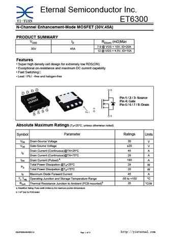
Eternal Semiconductor Inc. ET6300 N-Channel Enhancement-Mode MOSFET (30V,45A) PRODUCT SUMMARY VDSS ID RDS(on) (m )Max 7.9 @ VGS = 10V, ID=20A 30V 45A 12 @ VGS = 4.5V, ID=10A Features Super high density cell design for extremely low RDS(ON) Exceptional on-resistance and maximum DC current capability Fast Switching Lead Pb -free and halogen-free Pin 1 / 2 / 3 ... See More ⇒
et6309.pdf
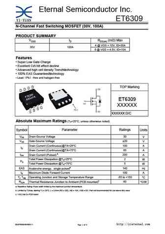
Eternal Semiconductor Inc. ET6309 N-Channel Fast Switching MOSFET (30V, 100A) PRODUCT SUMMARY VDSS ID RDS(on) (m ) Max 4 @ VGS = 10V, ID=30A 30V 100A 6 @ VGS = 4.5V, ID=15A Features Super Low Gate Charge Excellent CdV/dt effect decline Advanced high cell density Trenchtechnology 100% EAS Guaranteedtechnology Lead Pb -free and halogen-free TOP Marking E... See More ⇒
et6303.pdf
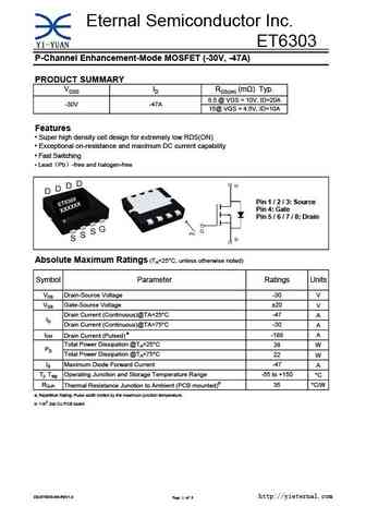
Eternal Semiconductor Inc. ET6303 P-Channel Enhancement-Mode MOSFET (-30V, -47A) PRODUCT SUMMARY VDSS ID RDS(on) (m ) Typ. 8.5 @ VGS = 10V, ID=20A -30V -47A 15@ VGS = 4.5V, ID=10A Features Super high density cell design for extremely low RDS(ON) Exceptional on-resistance and maximum DC current capability Fast Switching Lead Pb -free and halogen-free Pin 1 / 2 ... See More ⇒
et6304.pdf
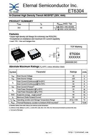
Eternal Semiconductor Inc. ET6304 N-Channel High Density Trench MOSFET (30V, 64A) PRODUCT SUMMARY VDSS ID RDS(on) (m ) Typ. 4 @ VGS = 10V, ID=20A 30V 64 5.7 @ VGS = 4.5V, ID=16A Features Super high density cell design for extremely low RDS(ON) Exceptional on-resistance and maximum DC current capability Lead Pb -free and halogen-free TOP Marking ET6304 XXXXXX ... See More ⇒
hssk6303.pdf
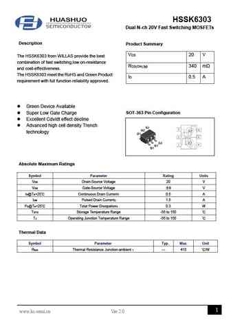
HSSK6303 Dual N-ch 20V Fast Switching MOSFETs Description Product Summary VDS 20 V The HSSK6303 from WILLAS provide the best combination of fast switching,low on-resistance RDS(ON),typ 340 m and cost-effectiveness. The HSSK6303 meet the RoHS and Green Product ID 0.5 A requirement with full function reliability approved. Green Device Available Super Low Gate C... See More ⇒
hsm6303.pdf
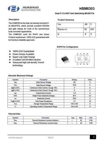
HSM6303 Dual P-Ch 60V Fast Switching MOSFETs Description Product Summary The HSM6303 is the high cell density trenched P- VDS -60 V ch MOSFETs, which provide excellent RDSON and gate charge for most of the synchronous RDS(ON),TYP 58 m buck converter applications. ID -4 A The HSM6303 meet the RoHS and Green Product requirement, 100% EAS guaranteed with full function re... See More ⇒
jmsl0630ag.pdf
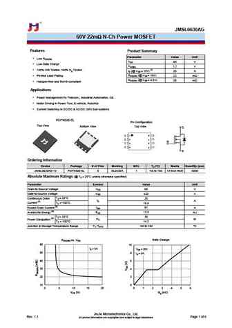
JMSL0630AG 60V 22m N-Ch Power MOSFET Features Product Summary Parameter Value Unit Low RDS(ON) VDS 60 V Low Gate Charge VGS(th) 1.7 V 100% UIS Tested, 100% Rg Tested ID (@ VGS = 10V) (1) 25 A RDS(ON) (@ VGS = 10V) Pb-free Lead Plating 22 m RDS(ON) (@ VGS = 4.5V) 28 m Halogen-free and RoHS-compliant Applications Power Managerment in Telecom.,... See More ⇒
jmsl0630au.pdf
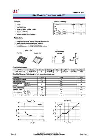
JMSL0630AU 60V 22m N-Ch Power MOSFET Features Product Summary Parameter Value Unit Low RDS(ON) VDS 60 V Low Gate Charge VGS(th) 1.7 V 100% UIS Tested, 100% Rg Tested ID (@ VGS = 10V) (1) 20 A RDS(ON) (@ VGS = 10V) Pb-free Lead Plating 22 m RDS(ON) (@ VGS = 4.5V) 30 m Halogen-free and RoHS-compliant Applications Power Managerment in Telecom.,... See More ⇒
jmsl0630agd.pdf
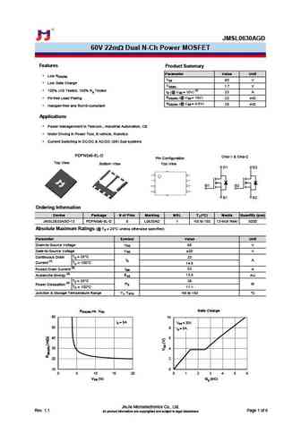
JMSL0630AGD 60V 22m Dual N-Ch Power MOSFET Features Product Summary Parameter Value Unit Low RDS(ON) VDS 60 V Low Gate Charge VGS(th) 1.7 V 100% UIS Tested, 100% Rg Tested ID (@ VGS = 10V) (1) 23 A RDS(ON) (@ VGS = 10V) Pb-free Lead Plating 22 m RDS(ON) (@ VGS = 4.5V) 28 m Halogen-free and RoHS-compliant Applications Power Managerment in ... See More ⇒
jmpf630bj.pdf
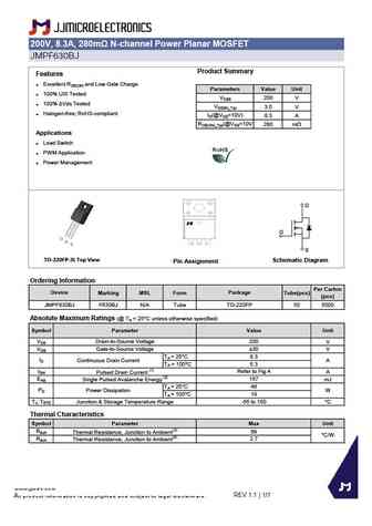
200V, 8.3A, 280m N-channel Power Planar MOSFET JMPF630BJ Product Summary Features Excellent RDS(ON) and Low Gate Charge Parameters Value Unit 100% UIS Tested VDSS 200 V 100% Vds Tested VGS(th)_Typ 3.0 V Halogen-free; RoHS-compliant ID(@VGS=10V) 8.3 A RDS(ON)_Typ(@VGS=10V 280 mW Applications Load Switch PWM Application Power Management D G S ... See More ⇒
jmpc630bj.pdf
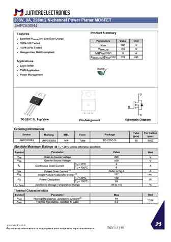
200V, 9A, 228m N-channel Power Planar MOSFET JMPC630BJ Product Summary Features Excellent RDS(ON) and Low Gate Charge Parameters Value Unit 100% UIS Tested VDSS 200 V 100% Vds Tested VGS(th)_Typ 2.9 V Halogen-free; RoHS-compliant ID(@VGS=10V) 9 A RDS(ON)_Typ(@VGS=10V 228 mW Applications Load Switch PWM Application Power Management D G S TO-2... See More ⇒
jmpk630bj.pdf
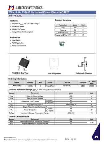
200V, 8.1A, 231m N-channel Power Planar MOSFET JMPK630BJ Product Summary Features Excellent RDS(ON) and Low Gate Charge Parameters Value Unit 100% UIS Tested VDSS 200 V 100% Vds Tested VGS(th)_Typ 3.0 V Halogen-free; RoHS-compliant ID(@VGS=10V) 8.1 A RDS(ON)_Typ(@VGS=10V 231 mW Applications Load Switch PWM Application Power Management D G S ... See More ⇒
se630k.pdf
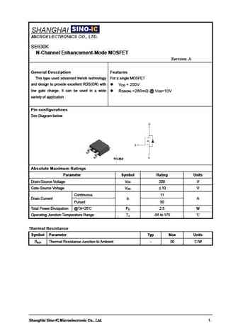
SE630K N-Channel Enhancement-Mode MOSFET Revision A General Description Features This type used advanced trench technology For a single MOSFET and design to provide excellent RDS(ON) with V = 200V DS low gate charge. It can be used in a wide R =260m @ V =10V DS(ON) GS variety of application Pin configurations See Diagram below TO-252 Absolute Maximum Ratings Parameter... See More ⇒
irlml6302trpbf.pdf
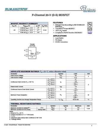
IRLML6302TRPBF www.VBsemi.tw P-Channel 20-V (D-S) MOSFET FEATURES MOSFET PRODUCT SUMMARY Halogen-free According to IEC 61249-2-21 VDS (V) RDS(on) ( )ID (A)a Qg (Typ.) Definition 0.035 at VGS = - 10 V - 5e TrenchFET Power MOSFET e - 20 0.043 at VGS = - 4.5 V - 5 10 nC 100 % Rg Tested 0.061 at VGS = - 2.5 V - 4.8 Compliant to RoHS Directive 2002/95/EC APPLICATI... See More ⇒
vbb1630.pdf
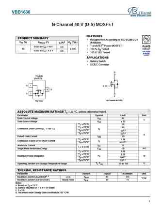
VBB1630 www.VBsemi.com N-Channel 60-V (D-S) MOSFET FEATURES PRODUCT SUMMARY Halogen-free According to IEC 61249-2-21 VDS (V) RDS(on) ( ) ID (A)a Qg (Typ.) Available TrenchFET Power MOSFET 0.030 at VGS = 10 V 5.5 60 2.3 nC 100 % Rg Tested 0.033 at VGS = 4.5 V 4.5 100 % UIS Tested APPLICATIONS Battery Switch DC/DC Converter D TO-236 (SOT23) G 1... See More ⇒
vbfb1630.pdf
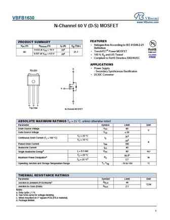
VBFB1630 www.VBsemi.com N-Channel 60 V (D-S) MOSFET FEATURES PRODUCT SUMMARY Halogen-free According to IEC 61249-2-21 VDS (V) RDS(on) ( ) ID (A) Qg (Typ.) Definition 0.032 at VGS = 10 V 35d TrenchFET Power MOSFET 60 21.7 0.037 at VGS = 4.5 V 30d 100 % Rg and UIS Tested Compliant to RoHS Directive 2002/95/EC APPLICATIONS Power Supply D TO-251 - Seconda... See More ⇒
irf630mfp.pdf
IRF630MFP www.VBsemi.tw N-Channel 200 V (D-S) MOSFET FEATURES PRODUCT SUMMARY Isolated Package VDS (V) 200 Available High Voltage Isolation = 2.5 kVRMS (t = 60 s; RDS(on) ( )VGS = 10 V 0.265 f = 60 Hz) RoHS Qg (Max.) (nC) 16 Sink to Lead Creepage Distance = 4.8 mm 175 C Operating Temperature Qgs (nC) 5 Dynamic dV/dt Rating Qgd (nC) 8 Low Thermal Resist... See More ⇒
fdc6305n.pdf
FDC6305N www.VBsemi.tw Dual N-Channel 20 V (D-S) MOSFET FEATURES PRODUCT SUMMARY Halogen-free According to IEC 61249-2-21 VDS (V) RDS(on) ( ) ID (A)a Qg (Typ.) Definition 0.022 at VGS = 4.5 V TrenchFET Power MOSFET 6.0 20 1.8 nC 100 % Rg Tested 0.028 at VGS = 2.5 V 5.0 Compliant to RoHS Directive 2002/95/EC TSOP-6 D1 D 2 D Top View G1 D1 1 6 G 1 ... See More ⇒
fds6630a.pdf
FDS6630A www.VBsemi.tw N-Channel 20V (D-S) MOSFET FEATURES PRODUCT SUMMARY Halogen-free VDS (V) RDS(on) ( ) ID (A)a Qg (Typ.) TrenchFET Power MOSFET 0.012 at VGS = 10 V 12 20 6.1 nC Optimized for High-Side Synchronous 0.015 at VGS = 4.5 V 11 Rectifier Operation 100 % Rg Tested 100 % UIS Tested APPLICATIONS Notebook CPU Core - High-Side Switch SO... See More ⇒
vbzm630.pdf
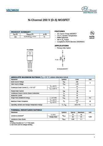
VBZM630 www.VBsemi.com N-Channel 200 V (D-S) MOSFET FEATURES PRODUCT SUMMARY DT-Trench Power MOSFET VDS (V) RDS(on) ( )ID (A) 175 C Junction Temperature 0.270 at VGS =10V 10 200 PWM Optimized 100 % Rg Tested Compliant to RoHS Directive 2002/95/EC APPLICATIONS Primary Side Switch TO-220AB D G S N-Channel MOSFET G D S Top View ABSOLUTE MAXIMUM RAT... See More ⇒
irf630p.pdf
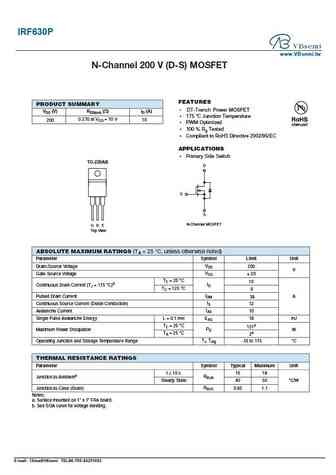
IRF630P www.VBsemi.tw N-Channel 200 V (D-S) MOSFET FEATURES PRODUCT SUMMARY DT-Trench Power MOSFET VDS (V) RDS(on) ( )ID (A) 175 C Junction Temperature 0.270 at VGS =10V 10 200 PWM Optimized 100 % Rg Tested Compliant to RoHS Directive 2002/95/EC APPLICATIONS Primary Side Switch TO-220AB D G S N-Channel MOSFET G D S Top View ABSOLUTE MAXIMUM RATI... See More ⇒
vbzm630y.pdf
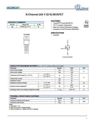
VBZM630Y www.VBsemi.com N-Channel 200 V (D-S) MOSFET FEATURES PRODUCT SUMMARY TrenchFET Power MOSFETS VDS (V) RDS(on) ( )ID (A) 175 C Junction Temperature RoHS 0.058at VGS =10V 35 200 COMPLIANT New Low Thermal Resistance Package Compliant to RoHS Directive 2002/95/EC APPLICATIONS TO-220AB Industrial D G G D S S N-Channel MOSFET ABSOLUTE MAXIMUM RA... See More ⇒
irf630s.pdf
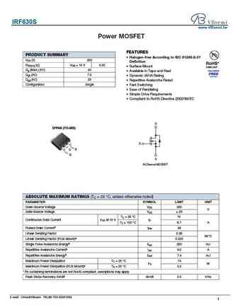
IRF630S www.VBsemi.tw Power MOSFET FEATURES PRODUCT SUMMARY Halogen-free According to IEC 61249-2-21 VDS (V) 200 Definition RDS(on) ( )VGS = 10 V 0.30 Surface Mount Qg (Max.) (nC) 43 Available in Tape and Reel Qgs (nC) 7.0 Dynamic dV/dt Rating Qgd (nC) 23 Repetitive Avalanche Rated Configuration Single Fast Switching Ease of Paralleling Simpl... See More ⇒
fdg6303n.pdf
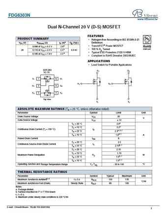
FDG6303N www.VBsemi.tw Dual N-Channel 20 V (D-S) MOSFET FEATURES PRODUCT SUMMARY Halogen-free According to IEC 61249-2-21 VDS (V) RDS(on) ( )ID (A)a Qg (Typ.) Definition TrenchFET Power MOSFET 0.086 at VGS = 4.5 V 2.6a 100 % Rg Tested 20 0.110 at VGS = 2.5 V 2.5a 5.0 nC Typical ESD Protection 2100 V HBM a 0.180 at VGS = 1.8 V 2.3 Compliant to RoHS Directive... See More ⇒
vba1630.pdf
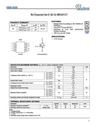
VBA1630 www.VBsemi.com N-Channel 60-V (D-S) MOSFET FEATURES PRODUCT SUMMARY Halogen-free According to IEC 61249-2-21 VDS (V) RDS(on) ( ) ID (A)d Qg (Typ.) Definition TrenchFET Power MOSFET 0.025 at VGS = 10 V 7.6 60 10.5 nC Optimized for Low Side Synchronous 0.030 at VGS = 4.5 V 6.5 Rectifier Operation 100 % Rg and UIS Tested APPLICATIONS D CCFL I... See More ⇒
fdn5630.pdf
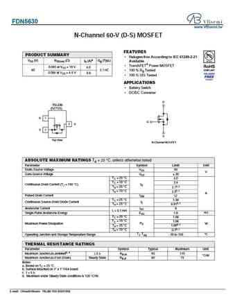
FDN5630 www.VBsemi.tw N-Channel 60-V (D-S) MOSFET FEATURES PRODUCT SUMMARY Halogen-free According to IEC 61249-2-21 VDS (V) RDS(on) ( ) ID (A)a Qg (Typ.) Available TrenchFET Power MOSFET 0.085 at VGS = 10 V 4.0 60 2.1 nC 100 % Rg Tested 0.096 at VGS = 4.5 V 3.8 100 % UIS Tested APPLICATIONS Battery Switch DC/DC Converter D TO-236 (SOT23) G 1 ... See More ⇒
hm4630d.pdf
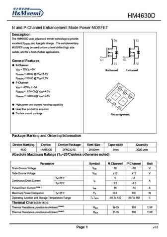
HM4630D N and P-Channel Enhancement Mode Power MOSFET Description The HM4630D uses advanced trench technology to provide excellent RDS(ON) and low gate charge . The complementary MOSFETs may be used to form a level shifted high side switch, and for a host of other applications. General Features N-Channel VDS = 30V,ID =5A N-channel P-channel RDS(ON) ... See More ⇒
ytf630.pdf
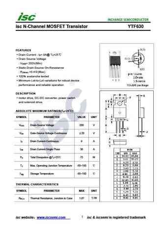
isc N-Channel MOSFET Transistor YTF630 FEATURES Drain Current I = 9A@ T =25 D C Drain Source Voltage V = 200V(Min) DSS Static Drain-Source On-Resistance R =0.4 (Max) DS(on) 100% avalanche tested Minimum Lot-to-Lot variations for robust device performance and reliable operation DESCRIPTION motor drive, DC-DC converter, power switch and solenoid drive. ABSOLU... See More ⇒
2n5629 2n5630.pdf
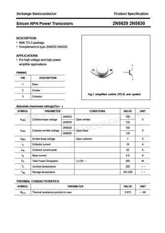
Inchange Semiconductor Product Specification Silicon NPN Power Transistors 2N5629 2N5630 DESCRIPTION With TO-3 package Complement to type 2N6029 2N6030 APPLICATIONS For high voltage and high power amplifier applications PINNING PIN DESCRIPTION 1 Base 2 Emitter Fig.1 simplified outline (TO-3) and symbol 3 Collector Absolute maximum ratings(Ta= ) SYMBOL PARAMETE... See More ⇒
irf630.pdf
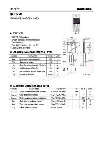
MOSFET INCHANGE IRF630 N-channel mosfet transistor Features 1 2 3 With TO-220 package Low on-state and thermal resistance Fast switching VDSS=200V; RDS(ON) 0.4 ;ID=9A 1.gate 2.drain 3.source Absolute Maximum Ratings Tc=25 SYMBOL PARAMETER RATING UNIT VDSS Drain-source voltage (VGS=0) 200 V VGS Gate-source voltage 20 V ID Drain Current-continuous@ TC... See More ⇒
2sk630.pdf
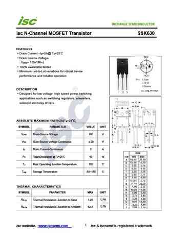
isc N-Channel MOSFET Transistor 2SK630 FEATURES Drain Current I =5A@ T =25 D C Drain Source Voltage- V = 160V(Min) DSS 100% avalanche tested Minimum Lot-to-Lot variations for robust device performance and reliable operation DESCRIPTION Designed for low voltage, high speed power switching applications such as switching regulators, converters, solenoid and relay dri... See More ⇒
2n6307.pdf
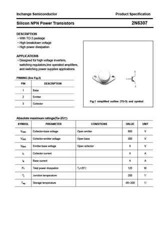
Inchange Semiconductor Product Specification Silicon NPN Power Transistors 2N6307 DESCRIPTION With TO-3 package High breakdown voltage High power dissipation APPLICATIONS Designed for high voltage inverters, switching regulators,line operated amplifiers, and switching power supplies applications PINNING (See Fig.2) PIN DESCRIPTION 1 Base 2 Emitter Fig.1 simplif... See More ⇒
mj6308.pdf
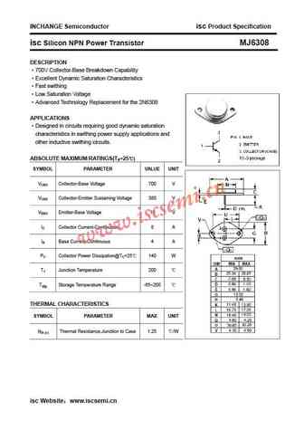
INCHANGE Semiconductor isc Product Specification isc Silicon NPN Power Transistor MJ6308 DESCRIPTION 700V Collector-Base Breakdown Capability Excellent Dynamic Saturation Characteristics Fast swithing Low Saturation Voltage Advanced Technology Replacement for the 2N6308 APPLICATIONS Designed in circuits requiring good dynamio saturation characteristics in swithin... See More ⇒
irf630b.pdf
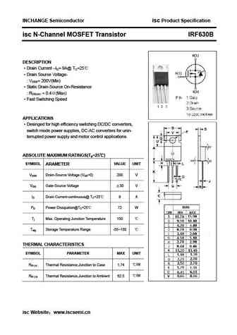
INCHANGE Semiconductor isc Product Specification isc N-Channel MOSFET Transistor IRF630B DESCRIPTION Drain Current ID= 9A@ TC=25 Drain Source Voltage- VDSS= 200V(Min) Static Drain-Source On-Resistance RDS(on) = 0.4 (Max) Fast Switching Speed APPLICATIONS Desinged for high efficiency switching DC/DC converters, switch mode power supplies, DC-AC conve... See More ⇒
2sk1630.pdf
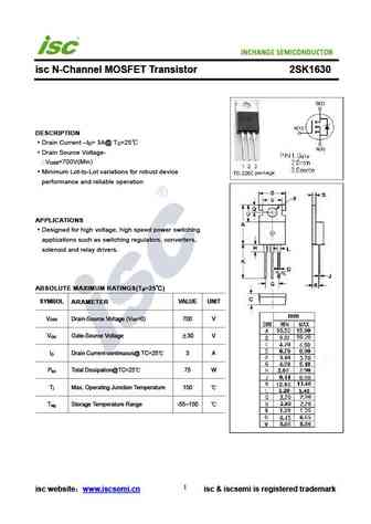
isc N-Channel MOSFET Transistor 2SK1630 DESCRIPTION Drain Current I = 3A@ T =25 D C Drain Source Voltage- V =700V(Min) DSS Minimum Lot-to-Lot variations for robust device performance and reliable operation APPLICATIONS Designed for high voltage, high speed power switching applications such as switching regulators, converters, solenoid and relay drivers. ABSOLUTE MAX... See More ⇒
2n6308.pdf
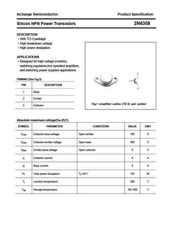
Inchange Semiconductor Product Specification Silicon NPN Power Transistors 2N6308 DESCRIPTION With TO-3 package High breakdown voltage High power dissipation APPLICATIONS Designed for high voltage inverters, switching regulators,line operated amplifiers, and switching power supplies applications PINNING (See Fig.2) PIN DESCRIPTION 1 Base 2 Emitter Fig.1 simplif... See More ⇒
2sb630.pdf
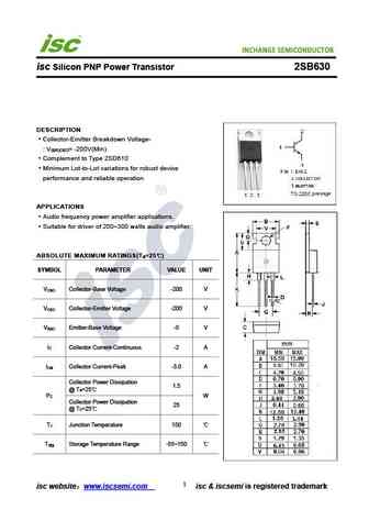
isc Silicon PNP Power Transistor 2SB630 DESCRIPTION Collector-Emitter Breakdown Voltage- V = -200V(Min) (BR)CEO Complement to Type 2SD610 Minimum Lot-to-Lot variations for robust device performance and reliable operation APPLICATIONS Audio frequency power amplifier applications. Suitable for driver of 200 300 watts audio amplifier. ABSOLUTE MAXIMUM RATINGS(T =25 ) a S... See More ⇒
2n6300 2n6301.pdf
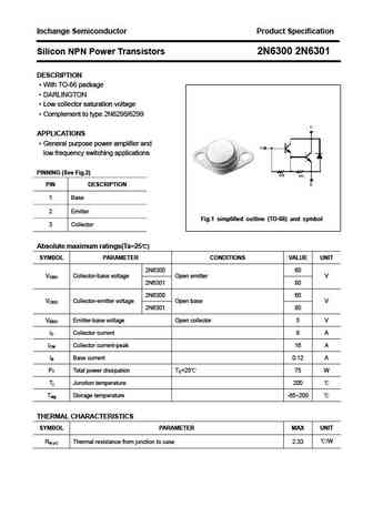
Inchange Semiconductor Product Specification Silicon NPN Power Transistors 2N6300 2N6301 DESCRIPTION With TO-66 package DARLINGTON Low collector saturation voltage Complement to type 2N6298/6299 APPLICATIONS General purpose power amplifier and low frequency switching applications PINNING (See Fig.2) PIN DESCRIPTION 1 Base 2 Emitter Fig.1 simplified outline (T... See More ⇒
irf630a.pdf
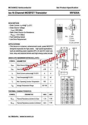
INCHANGE Semiconductor isc Product Specification isc N-Channel MOSFET Transistor IRF630A DESCRIPTION Drain Current ID=9A@ TC=25 Drain Source Voltage- VDSS= 200V(Min) Static Drain-Source On-Resistance RDS(on) = 0.4 (Max) Fast Switching Speed Low Drive Requirement APPLICATIONS This device is n-channel, enhancement mode, power MOSFET designed espec... See More ⇒
irf630nl.pdf
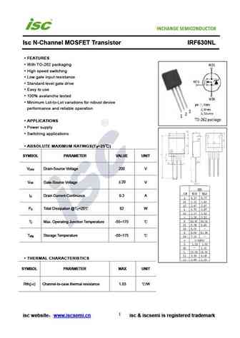
Isc N-Channel MOSFET Transistor IRF630NL FEATURES With TO-262 packaging High speed switching Low gate input resistance Standard level gate drive Easy to use 100% avalanche tested Minimum Lot-to-Lot variations for robust device performance and reliable operation APPLICATIONS Power supply Switching applications ABSOLUTE MAXIMUM RATINGS(T =25 ) a SYMBOL PAR... See More ⇒
irlml6302.pdf
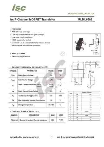
Isc P-Channel MOSFET Transistor IRLML6302 FEATURES With SOT-23 package Low input capacitance and gate charge Low gate input resistance 100% avalanche tested Minimum Lot-to-Lot variations for robust device performance and reliable operation APPLICATIONS Switching applications ABSOLUTE MAXIMUM RATINGS(T =25 ) a SYMBOL PARAMETER VALUE UNIT V Drain-Source Voltage -2... See More ⇒
irf630nstrrpbf.pdf
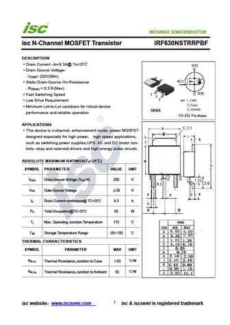
INCHANGE Semiconductor isc N-Channel MOSFET Transistor IRF630NSTRRPBF DESCRIPTION Drain Current I =9.3A@ T =25 D C Drain Source Voltage- V = 200V(Min) DSS Static Drain-Source On-Resistance R = 0.3 (Max) DS(on) Fast Switching Speed Low Drive Requirement Minimum Lot-to-Lot variations for robust device performance and reliable operation APPLICATIONS This de... See More ⇒
irf630ns.pdf
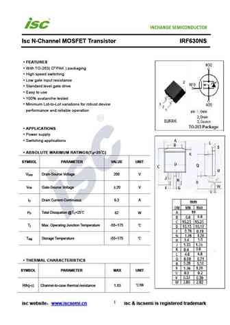
Isc N-Channel MOSFET Transistor IRF630NS FEATURES With TO-263( D PAK ) packaging High speed switching Low gate input resistance Standard level gate drive Easy to use 100% avalanche tested Minimum Lot-to-Lot variations for robust device performance and reliable operation APPLICATIONS Power supply Switching applications ABSOLUTE MAXIMUM RATINGS(T =25 ) a ... See More ⇒
2n6302.pdf
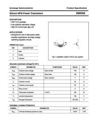
Inchange Semiconductor Product Specification Silicon NPN Power Transistors 2N6302 DESCRIPTION With TO-3 package Low collector saturation voltage High DC current gain @IC=8A APPLICATIONS Designed for use in high power audio amplifier applications and high voltage switching regulator circuits PINNING (See Fig.2) PIN DESCRIPTION 1 Base 2 Emitter Fig.1 simplified ... See More ⇒
irf630n.pdf
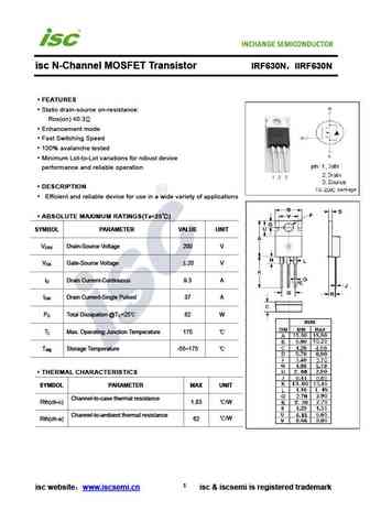
isc N-Channel MOSFET Transistor IRF630N IIRF630N FEATURES Static drain-source on-resistance RDS(on) 0.3 Enhancement mode Fast Switching Speed 100% avalanche tested Minimum Lot-to-Lot variations for robust device performance and reliable operation DESCRIPTION Efficient and reliable device for use in a wide variety of applications ABSOLUTE MAXIMUM RATINGS(T ... See More ⇒
2n6306.pdf
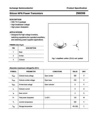
Inchange Semiconductor Product Specification Silicon NPN Power Transistors 2N6306 DESCRIPTION With TO-3 package High breakdown voltage High power dissipation APPLICATIONS Designed for high voltage inverters, switching regulators,line operated amplifiers, and switching power supplies applications PINNING (See Fig.2) PIN DESCRIPTION 1 Base 2 Emitter Fig.1 simplif... See More ⇒
irf630f.pdf
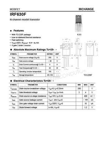
MOSFET INCHANGE IRF630F N-channel mosfet transistor Features With TO-220F package 1 2 3 Low on-stateand thermal resistance Fast switching VDSS=200V; RDS(ON) 0.4 ;ID=9A 1.gate 2.drain 3.source Absolute Maximum Ratings Tc=25 SYMBOL PARAMETER RATING UNIT VDSS Drain-source voltage (VGS=0) 200 V VGS Gate-source voltage 20 V ID Drain Current-continuous@ TC... See More ⇒
Detailed specifications: FXN4N65D, FXN7N65D, CRJQ99N65G2, LSD07N80A-VB, FXN0204C, FXN0204CQ, FXN100S55T, FXN9N20C, RFP50N06, 110N04, 13N90, 14N65, 18N50D, D2N60, D4N70, D4N80, D50N06
Keywords - 630 MOSFET specs
630 cross reference
630 equivalent finder
630 pdf lookup
630 substitution
630 replacement
Need a MOSFET replacement? Our guide shows you how to find a perfect substitute by comparing key parameters and specs
