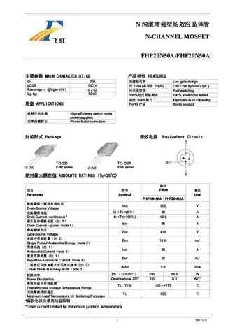
F20N50 Datasheet. Specs and Replacement
Type Designator: F20N50 📄📄
Type of Transistor: MOSFET
Type of Control Channel: N-Channel
Absolute Maximum Ratings
Pd ⓘ - Maximum Power Dissipation: 45 W
|Vds|ⓘ - Maximum Drain-Source Voltage: 500 V
|Vgs|ⓘ - Maximum Gate-Source Voltage: 30 V
|Id| ⓘ - Maximum Drain Current: 20 A
Tj ⓘ - Maximum Junction Temperature: 150 °C
Electrical Characteristics
tr ⓘ - Rise Time: 65 nS
Cossⓘ - Output Capacitance: 277 pF
RDSonⓘ - Maximum Drain-Source On-State Resistance: 0.3 Ohm
Package: TO220F
📄📄 Copy
- MOSFET ⓘ Cross-Reference Search
F20N50 datasheet
..1. Size:1374K cn wxdh
f20n50.pdf 
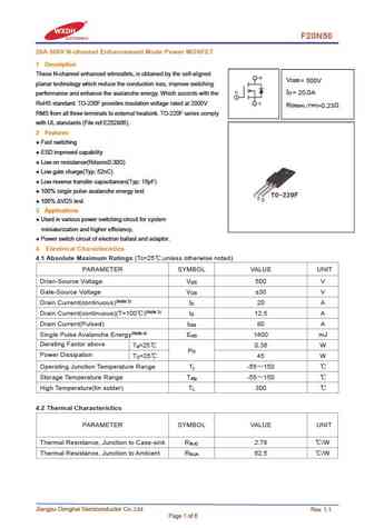
F20N50 20A 500V N-channel Enhancement Mode Power MOSFET 1 Description These N-channel enhanced vdmosfets, is obtained by the self-aligned V DSS = 500V planar technology which reduce the conduction loss, improve switching I = 20.0A D performance and enhance the avalanche energy. Which accords with the RoHS standard. TO-220F provides insulation voltage rated at 2000V R DS(on) TYP) ... See More ⇒
..2. Size:1298K cn wxdh
20n50 f20n50 i20n50 e20n50.pdf
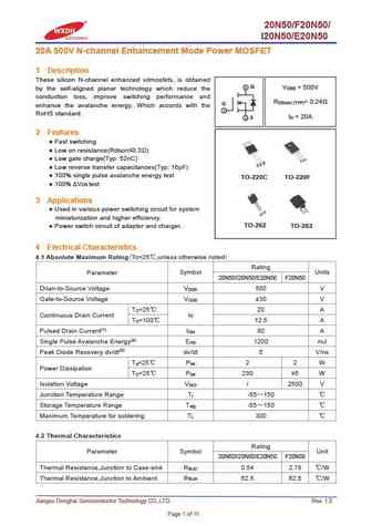
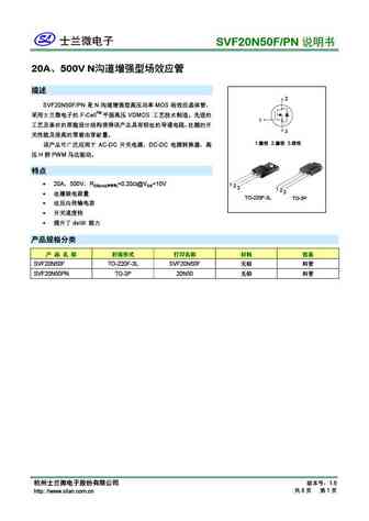
20N50/F20N50/ I20N50/E20N50 20A 500V N-channel Enhancement Mode Power MOSFET 1 Description These silicon N-channel enhanced vdmosfets, is obtained 2 D V = 500V DSS by the self-aligned planar technology which reduce the conduction loss, improve switching performance and R = 0.24 DS(on) (TYP) G enhance the avalanche energy. Which accords with the 1 RoHS standard. I = 20A 3 S D ... See More ⇒
0.1. Size:838K fairchild semi
fdp20n50f fdpf20n50ft.pdf
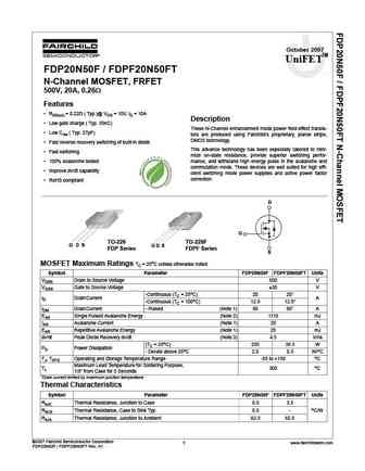
October 2007 UniFETTM FDP20N50F / FDPF20N50FT tm N-Channel MOSFET, FRFET 500V, 20A, 0.26 Features RDS(on) = 0.22 ( Typ.)@ VGS = 10V, ID = 10A Description Low gate charge ( Typ. 50nC) These N-Channel enhancement mode power field effect transis- Low Crss ( Typ. 27pF) tors are produced using Fairchild s proprietary, planar stripe, DMOS technology. Fast reve... See More ⇒
0.2. Size:469K fairchild semi
fdp20n50 fdpf20n50.pdf
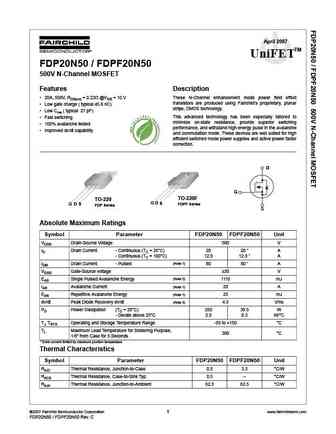
April 2007 TM UniFET FDP20N50 / FDPF20N50 500V N-Channel MOSFET Features Description 20A, 500V, RDS(on) = 0.23 @VGS = 10 V These N-Channel enhancement mode power field effect transistors are produced using Fairchild s proprietary, planar Low gate charge ( typical 45.6 nC) stripe, DMOS technology. Low Crss ( typical 27 pF) This advanced technology has been especially... See More ⇒
0.3. Size:665K fairchild semi
fdp20n50 fdpf20n50 fdpf20n50t.pdf
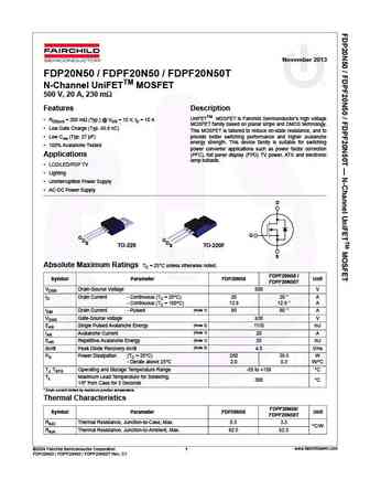
November 2013 FDP20N50 / FDPF20N50 / FDPF20N50T N-Channel UniFETTM MOSFET 500 V, 20 A, 230 m Features Description UniFETTM MOSFET is Fairchild Semiconductor s high voltage RDS(on) = 200 m (Typ.) @ VGS = 10 V, ID = 10 A MOSFET family based on planar stripe and DMOS technology. Low Gate Charge (Typ. 45.6 nC) This MOSFET is tailored to reduce on-state resistance, and to ... See More ⇒
0.4. Size:494K onsemi
fdp20n50f fdpf20n50ft.pdf

Is Now Part of To learn more about ON Semiconductor, please visit our website at www.onsemi.com Please note As part of the Fairchild Semiconductor integration, some of the Fairchild orderable part numbers will need to change in order to meet ON Semiconductor s system requirements. Since the ON Semiconductor product management systems do not have the ability to manage part nomenclatur... See More ⇒
0.5. Size:772K onsemi
fdp20n50 fdpf20n50 fdpf20n50t.pdf

Is Now Part of To learn more about ON Semiconductor, please visit our website at www.onsemi.com Please note As part of the Fairchild Semiconductor integration, some of the Fairchild orderable part numbers will need to change in order to meet ON Semiconductor s system requirements. Since the ON Semiconductor product management systems do not have the ability to manage part nomenclatur... See More ⇒
0.6. Size:463K silikron
ssf20n50uh.pdf
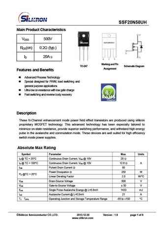
SSF20N50UH Main Product Characteristics VDSS 500V RDS(on) 0.2 (typ.) ID 20A Marking and Pi n TO-247 Schematic Diagram Assignment Features and Benefits Advanced Process Technology Special designed for PWM, load switching and general purpose applications Ultra low on-resistance with low gate charge Fast switching and reverse body recovery Descri... See More ⇒
0.7. Size:781K blue-rocket-elect
brf20n50.pdf
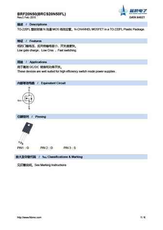
BRF20N50(BRCS20N50FL) Rev.C Feb.-2015 DATA SHEET / Descriptions TO-220FL N MOS N-CHANNEL MOSFET in a TO-220FL Plastic Package. / Features Low gate charge Low Crss Fast switching. / Applications DC/DC These devices a... See More ⇒
0.9. Size:843K bruckewell
msf20n50.pdf

MSF20N50 N-Channel Enhancement Mode Power MOSFET Description The MSF20N50 is a N-channel enhancement-mode MOSFET , providing the designer with the best combination of fast switching, ruggedized device design, low on-resistance and cost effectiveness. The TO-220F package is universally preferred for all commercial-industrial applications Features Low On Resistance S... See More ⇒
0.11. Size:1295K maple semi
slp20n50c slf20n50c.pdf
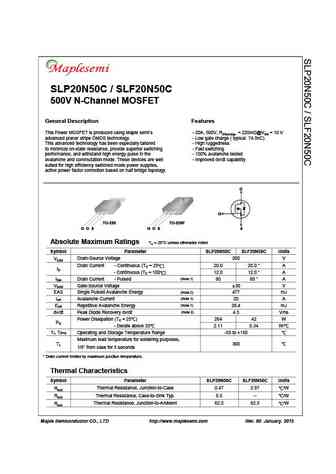
SLP20N50C / SLF20N50C 500V N-Channel MOSFET General Description Features This Power MOSFET is produced using Maple semi s - 20A, 500V, RDS(on)typ. = 220m @VGS = 10 V advanced planar stripe DMOS technology. - Low gate charge ( typical 74.5nC) This advanced technology has been especially tailored - High ruggedness to minimize on-state resistance, provide superior switching - Fast switchi... See More ⇒
0.12. Size:803K samwin
swf20n50d swt20n50d.pdf
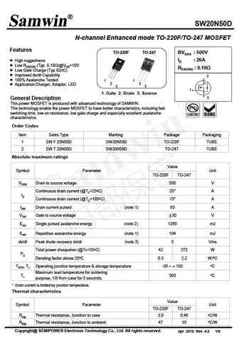
SW20N50D N-channel Enhanced mode TO-220F/TO-247 MOSFET Features TO-220F TO-247 BVDSS 500V ID 20A High ruggedness Low RDS(ON) (Typ 0.19 )@VGS=10V RDS(ON) 0.19 Low Gate Charge (Typ 82nC) Improved dv/dt Capability 2 100% Avalanche Tested 1 1 2 2 Application Charger, Adaptor, LED 3 3 1 1. Gate 2. Drain 3. Source 3 General De... See More ⇒
0.13. Size:409K trinnotech
tmp20n50 tmpf20n50.pdf
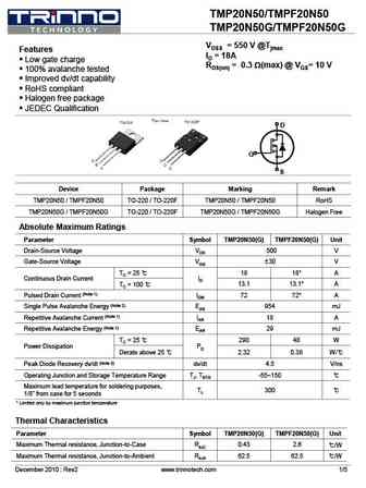
TMP20N50/TMPF20N50 TMP20N50G/TMPF20N50G VDSS = 550 V @Tjmax Features ID = 18A Low gate charge RDS(on) = 0.3 W(max) @ VGS= 10 V 100% avalanche tested Improved dv/dt capability RoHS compliant Halogen free package JEDEC Qualification D G S Device Package Marking Remark TMP20N50 / TMPF20N50 TO-220 / TO-220F TMP20N50 / TMPF20N50 RoHS TMP20N50... See More ⇒
0.14. Size:621K trinnotech
tmp20n50a tmpf20n50a.pdf
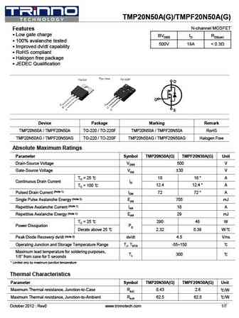
TMP20N50A(G)/TMPF20N50A(G) N-channel MOSFET Features Low gate charge BVDSS ID RDS(on) 100% avalanche tested 500V 18A ... See More ⇒
0.15. Size:802K truesemi
tsf20n50m.pdf
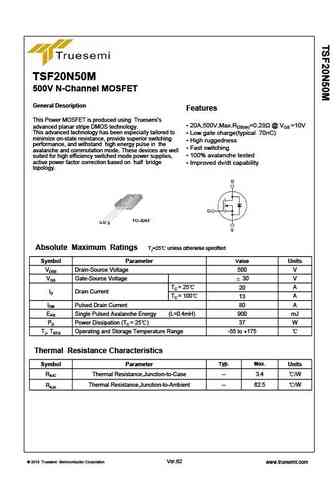
TSF20N50M 500V N-Channel MOSFET General Description Features This Power MOSFET is produced using Truesemi s 20A,500V,Max.RDS(on)=0.28 @ VGS =10V advanced planar stripe DMOS technology. This advanced technology has been especially tailored to Low gate charge(typical 70nC) minimize on-state resistance, provide superior switching High ruggedness performance, and withstan... See More ⇒
0.16. Size:4735K haolin elec
hf20n50 hp20n50.pdf
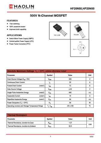
HF20N50,HP20N50 500V N-Channel MOSFET FEATURES Fast switching 100% avalanche tested Improved dv/dt capability APPLICATIONS Switch Mode Power Supply (SMPS) Uninterruptible Power Supply (UPS) Power Factor Correction (PFC) Absolute Maximum Ratings TC = 25 unless otherwise noted C, Parameter Symbol Value Unit Drain-Source Voltage (VGS = 0V) VDSS 500 V Continu... See More ⇒
0.17. Size:795K cn minos
mpf20n50.pdf
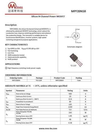
Silicon N-Channel Power MOSFET Description MPF20N50, the silicon N-channel Enhanced MOSFETS, is obtained by advanced MOSFET technology which reduce the conduction loss, improve switching performance and enhance the avalanche energy. The transistor is suitable device for Synchronous Rectification, inverter systems ,high speed switching and general purpose applications. KEY CHARACTERISTIC... See More ⇒
Detailed specifications: DTG050P06LA, DTJ018N04N, F12N60, F13N50, F14N65, F16N65, F18N50, F18N65, IRFB7545, F20N60, F25N10, DHS042N15, DHS042N15E, DHS042N85P, DHS043N07P, DHS043N85P, DHS044N12
Keywords - F20N50 MOSFET specs
F20N50 cross reference
F20N50 equivalent finder
F20N50 pdf lookup
F20N50 substitution
F20N50 replacement
Learn how to find the right MOSFET substitute. A guide to cross-reference, check specs and replace MOSFETs in your circuits.